


News: Microelectronics
27 November 2025
Nitrogen-polar III-N HFETs on 200mm sapphire substrates
RWTH Aachen University and AIXTRON SE in Germany have reported metal-organic chemical vapor deposition (MOCVD) growth of nitrogen-polar III-nitride layers on 200mm-diameter sapphire substrates, along with the fabrication of heterostructure field-effect transistors (HFETs) [Liubou Padzialioshkina et al, Appl. Phys. Lett., v127, p173302, 2025]
N-polar HFETs are expected to provide performance and scaling advantages over devices fabricated on metal-polar materials. MOCVD is the preferred industrial III-nitride growth method over molecular beam epitaxy to provide materials for cost-effective, large-scale fabrication. Previous N-polar growth reports have been limited to substrate sizes only up to 100mm.
Gallium nitride (GaN) in Ga-polar crystal orientation is simpler to grow at high quality and with superior chemical stability. Despite this, “more recent development efforts have been directed toward N-polar GaN growth, since HFETs with such inverted crystal orientation promise further performance and scaling advantages over Ga-polar ones,” the RWTH/AIXTRON team reports.
The inverted N-polar structure places the aluminium gallium nitride (AlGaN) layer below the GaN channel layer, with the conducting two-dimensional electron gas (2DEG) just above the barrier, improving carrier confinement and blocking current leaks into the buffer. The ohmic source/drain contacts can be made directly with the narrower-bandgap GaN, rather than with AlGaN, reducing contact resistance. With the channel layer rather than the barrier on top, the gate can be brought closer to the 2DEG channel, improving electrostatic control. N-polar HFETs have been reported with cut-off frequencies up to 132GHz.
The researchers used AIXTRON’s G5+C 5x200mm Planetary MOCVD reactor to perform N-polar III-nitride growth on 200mm-diameter sapphire substrates, offcut 2° towards the m-plane (Figure 1). The substrate was 1.3mm thick. The GaN channel thickness was varied on different wafers: 15nm, 25nm and 35nm.
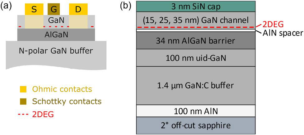
Figure 1: (a) Simple N-polar HFET scheme. (b) Investigated N-polar MOCVD layer stack.
The buffer layer was doped with carbon (C) with a view to compensate for background impurities, such as silicon (Si) and oxygen (O). Oxygen incorporation is a particular problem in N-polar MOCVD growth. The AlGaN layer was grown on an unintentionally doped (uid) GaN layer, designed to isolate the C acceptors in the buffer from the active region of the device. The pseudomorphic (fully strained) barrier layer contained 32% Al.
The structure was capped with in-situ silicon nitride (SiN). The researchers comment: “Wafers without in-situ SiN exhibit a non-coalesced surface likely originating from H2-induced GaN etching during the cooldown process. In-situ SiN passivation ensures smooth topology of the wafers and is, therefore, featured in all processed samples.”
Double-finger HFETs were fabricated (Figure 2). Most of the devices included ex-situ plasma-enhanced CVD (PECVD) SiN. Patterning used optical lithography.
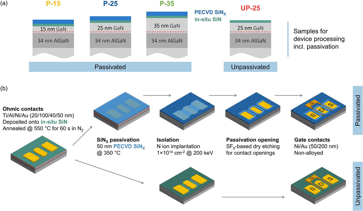
Figure 2: (a) Overview of samples and (b) fabrication sequence chart.
The ex-situ passivation was found to be necessary to yield high channel layer mobilities of around 1000cm2/V-s in the P-25 and P-35 samples. Without passivation, the UP-25 sample had a factor-of-three reduction in mobility at 300cm2/V-s.
The researchers report: “Corresponding sheet resistance values extracted from the Hall measurement are on average 5000Ω/sq, 550Ω/sq, 500Ω/sq and 2500Ω/sq for P-15, P-25, P-35 and UP-25, respectively.”
The ohmic contacts, titanium/aluminium/nickel/gold (Al/Ti/Ni/Au), were annealed at the relatively low temperature of 550°C, which has been found to yield the lowest contact resistance on N-polar structures, according to previous work by the team. The ex-situ passivation was performed before gate formation to avoid unintentional annealing of the gate contact. Device isolation was by nitrogen ion implantation.
The gate width was 2x50μm, and the 1μm-long gate was placed at 1.5μm from the source contact, and 2.5μm from the drain.
The researchers comment: “It should be noted that, due to a high surface roughness, sufficient photoresist adhesion and uniform exposure during the lithography process remain challenging. This potentially results in deviations from the nominal gate length and distance values from device to device.”
The ex-situ passivation increased the average peak transconductance (gm) for 25nm thick channel layers from 100mS/mm to 130mS/mm (Figure 3). The best P-25 device reached 150mS/mm. The researchers mainly attribute this to the much lower sheet resistance of the P-25 material: 550Ohm/square compared with 2500Ohm/square.
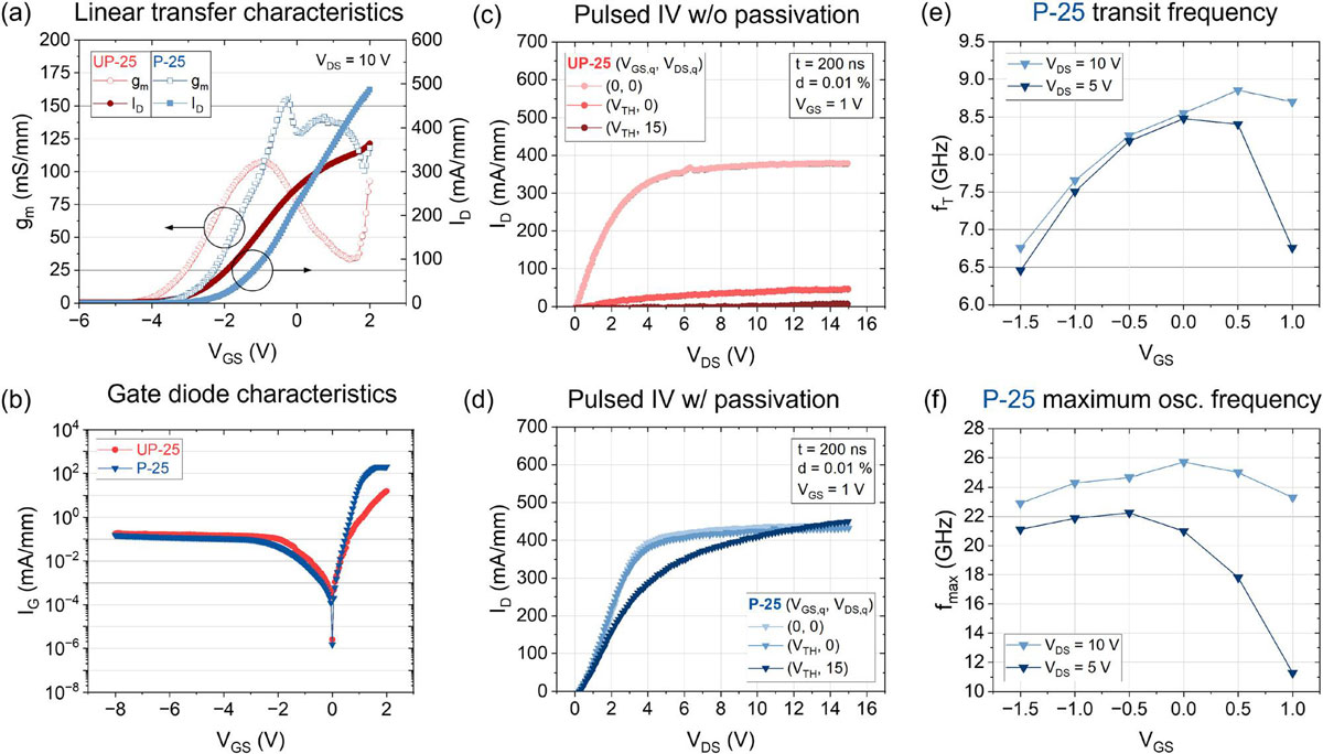
Figure 3: Representative linear transfer characteristics (a) and gate diode current–voltage (IV) characteristics (b) of unpassivated (UP-25) and passivated (P-25) HFETs at 10V drain bias (VDS). Pulsed-IV output characteristics for UP-25 (c) and P-25 (d) HFETs at 1V gate potential (VGS). Transit (e) and maximum oscillation frequency (f) extracted from small-signal measurements of P-25 HFET.
The researchers report that “the reverse-bias gate leakage currents are rather high in fabricated HFETs, as expected from the lower Schottky barrier height (SBH) values.” Even the best devices only manage a 103 on/off current ratio.
Ex situ passivation also reduced current collapse under pulsed operation, from 97% to 7%. The team concludes that “in-situ SiN is not sufficient for passivation, while ex-situ SiNX, including ammonia (NH3) plasma treatment, effectively passivates the surface trap states responsible for the DC–RF dispersion.”
Small-signal frequency measurements resulted in transit (fT) and maximum oscillation (fmax) frequencies up to 9GHz and 26GHz, respectively, for P-25 HFETs.
The team comments: “Considering the nominal gate-length value of 1μm, the transit-frequency x gate-length product is calculated to be fT x LG = 9 GHzxμm. Typically reported values for N-polar HFETs start from 8GHzxμm, with the state-of-the-art short-channel devices reaching as high as 16GHzxμm.”
Looking to the future, the researchers comment: “Further optimization of N-polar epitaxial quality is required to improve uniformity, minimize surface roughness, and reduce leakage currents.”
Nitrogen-polar III-N HFETs Sapphire substrates Aixtron MOCVD GaN
https://doi.org/10.1063/5.0299401
The author Mike Cooke is a freelance technology journalist who has worked in the semiconductor and advanced technology sectors since 1997.


