


News: Suppliers
15 May 2025
Mass production QF-HVPE of GaN-on-GaN system
Sumitomo Chemical Co Ltd in Japan has developed a mass-production quartz-free hydride vapor phase epitaxy (QF-HVPE) system capable of fabricating gallium nitride (GaN) with a claimed record mobility both at room temperature and low temperature [Shota Kaneki et al, Appl. Phys. Express, v18, p055502, 2025]. The material was demonstrated both on 4-inch freestanding GaN substrates and 6-inch GaN-on-sapphire templates.
The Sumitomo team was particularly concerned to reduce carbon contamination, which has been associated with mobility collapse below theoretical expectations. HVPE avoids the presence of carbon that is unavoidable in the metal-organic (MO)VPE conventionally used in growing high-quality GaN layers in mass production. Avoiding quartz (crystalline SiO4) in the system construction enables better control of silicon (Si) doping used to achieve n-type, electron majority transport.
The team suggest that their work could lead to GaN-on-GaN power devices for applications that require breakdown voltages greater than 10kV, as needed for power drive and inverter systems used in electric vehicles and drones.
The team describes the motivation for the switch to electric-powered transportation: “Achieving carbon neutrality is strongly demanded for realizing the sustainable development goals developed in response to the rapid progression of global warming, which has led to frequent extreme weather and disasters around the world in recent years. Because thermal power generation accounts for more than 60% of the world’s electricity generation, the proliferation of renewable energy and the reduction of losses through high-efficiency power conversion systems are essential to achieve carbon neutrality.”
GaN has a wide bandgap that enables high breakdown voltages in semiconductor device structures.
Figure 1: Six-inch GaN template on sapphire substrate fabricated using QF-HVPE system.
The QF-HVPE was performed at 1050°C, giving a growth rate of 1μm/minute. This compares very favorably relative to the typical μms/hour rates for MOVPE. The Ga and N chemical elements were sourced from ammonia (NH3) and gallium monochloride (GaCl). Dichlorosilane (H2SiCl2) was used for Si doping. These active components were carried to the growth front in a mix of hydrogen and nitrogen gases. The researchers grew GaN layers with a target 4x10¹⁵/cm3 silicon concentration ([Si]) on substrates with 4- and 6-inch diameters. The 4-inch substrate was freestanding GaN, while the 6-inch-diameter layer was grown on a GaN-on-sapphire template (Figure 1).
The researchers used secondary-ion mass spectroscopy (SIMS) to show that the mass-production QF-HVPE system eliminated carbon and oxygen contaminations as far as possible. In particular, the concentrations of these two elements was found to be below the detection limits of their analysis: 1x10¹⁴/cm3 for [C], and 5x10¹⁴/cm3 for [O]. The researchers comment that this improves on a prototype QF-HVPE system reported in early 2024 that managed to reduce carbon contamination to a just measurable 1.4x10¹⁴/cm3.
The researchers report: “Each sample exhibited almost featureless surfaces without pits or hillocks and a smooth as-grown surface with regularly arranged steps, as evaluated from an atomic force microscopy image and consistent with previous reports. Because the surface morphology directly affects the leakage current of devices, this flat surface without pits and hillocks is favorable for the stable operation of GaN devices.”
According to Fourier transform infrared (FTIR) spectral analysis the layers were 14.1μm thick. Unlike conventional HVPE, which suffers from large thickness variations, the Sumitomo researchers found that their layer thicknesses had just 3.4% standard deviation, “similar to that of an MOVPE-grown epitaxial film”. The growth on the 6-inch GaN/sapphire template had a larger, but “reasonable” thickness standard deviation of 4.4%. The team reports that 6-inch freestanding GaN substrates are under development.
The excess of donors over acceptors (ND–NA) in the material was assessed using non-contact capacitance–voltage (C–V) measurements. Samples grown with metal-organic vapor phase epitaxy (MOVPE) had average ND–NA values of 4.3x10¹⁵/cm3, compared with 6.8x10¹⁵/cm3 for the QF-HVPE sample. The MOVPE sample suffered from a high variability of ND–NA with 14.3% standard deviation. By contrast the standard deviation for the QF-HVPE GaN layer on 4-inch freestanding substrate was only 3.0%. The team suggests that the problem for the MOVPE sample was the off-angle-dependent C-incorporation efficiency, based on previous work. The carbon-free nature of the QF-HVPE avoids this problem.
The control of carrier concentration was demonstrated by varying [Si] during the last 2.4μm growth in 600nm steps (Figure 2). The dependence ND–NA on [Si] was found to be linear over the wide range 1014–1018/cm3.
![Figure 2: (a) Depth profile of [Si] obtained by SIMS analysis, [Si] varied stepwise every 600nm; epitaxial layer deeper than 2.4μm from surface was unintentionally doped. (b) Relationship between [Si] and ND–NA of QF-HVPE-grown layer on freestanding GaN substrate from non-contact C–V analysis.](25052_sumitomo_f2.jpg)
Figure 2: (a) Depth profile of [Si] obtained by SIMS analysis, [Si] varied stepwise every 600nm; epitaxial layer deeper than 2.4μm from surface was unintentionally doped. (b) Relationship between [Si] and ND–NA of QF-HVPE-grown layer on freestanding GaN substrate from non-contact C–V analysis.
The researchers comment: “Control of the carrier concentration in epitaxial layers grown by MOVPE is known to be poor when the carrier concentration is less than 1x10¹⁶/cm3 because of C-induced carrier compensation. On the contrary, the high purity of QF-HVPE-grown layers, in which the C contaminant concentration was less than 1x10¹⁴/cm3, led to high linearity even at carrier concentrations less than 1x10¹⁶/cm3. Given that many power devices operate at voltages above the kilovolt range, controlling the carrier concentration in the concentration range below 1x10¹⁶/cm3 is essential.”
Hall-effect measurements (Figure 3) showed record mobility values at room temperature (295K) and low temperature (35K) of 1591cm2/V-s and 18,175cm2/V-s, respectively.
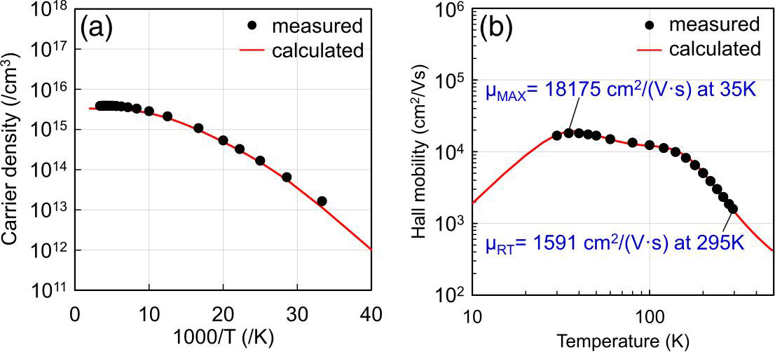
Figure 3: Measured and calculated temperature dependence of (a) carrier density and (b) Hall mobility for QF-HVPE-grown GaN bulk crystal. Black closed circles and red solid lines represent acquired data with curves fitted using traditional mobility theory.
The researchers comment: “Although various research groups, including our group, have reported an anomalous decrease of the electron mobility in GaN layers compared with the theoretical value — a phenomenon known as mobility collapse — the present data can be well fitted using the traditional mobility theory.”
The mobility collapse has been explained by C-induced scattering, and Sumitomo’s results on its low [C] material supports this assertion. Photoluminescence experiments also showed spectra without blue and yellow emissions associated with carbon contamination.
https://doi.org/10.35848/1882-0786/adce53
https://www.semiconductor-today.com
The author Mike Cooke is a freelance technology journalist who has worked in the semiconductor and advanced technology sectors since 1997.


