


News: Suppliers
1 May 2025
Beneq Transform ALD cluster tool qualified for GaN power device production by tier-1 Asian manufacturer
Beneq of Espoo, Finland says that its Transform atomic layer deposition (ALD) cluster tool has been qualified for volume production of gallium nitride (GaN)-based power devices on 8-inch GaN-on-silicon wafers by a tier-1 GaN power device manufacturer in Asia.
The system enables a proprietary three-step process - plasma-based surface pre-cleaning, plasma-enhanced ALD (PEALD) of interfacial layers, and thermal ALD of dielectric films — executed under continuous vacuum. This architecture is said to ensure high-quality interface engineering and process reliability, which is critical for wide-bandgap materials such as GaN and silicon carbide (SiC). Additional capabilities include nitride film deposition (e.g. AlN, SiN) and thermal ALD of films such as Al2O3, AlN, SiO2 and HfO2, offering flexibility across GaN high-electron-mobility transistors (HEMTs), ICs and vertical devices.
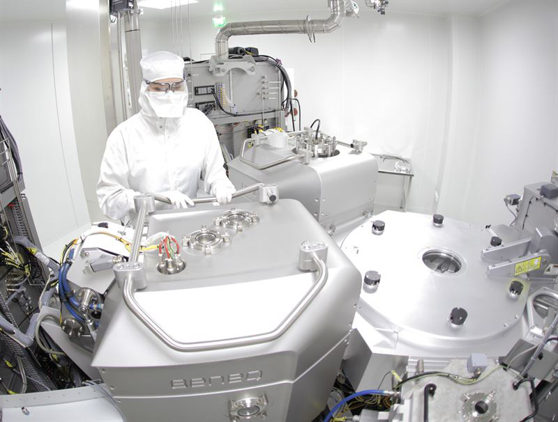
The vacuum-integrated cluster tool design features high throughput andwhat is claimed to be best-in-class cost-of-ownership while supporting demanding process requirements. Seventeen Beneq Transform tools are now in operation globally for GaN device production and technology development.
“Qualification by a tier-1 GaN power device manufacturer underscores the strength of our Transform platform and its leading role in GaN manufacturing,” says Pasi Meriläinen, VP Semiconductor ALD at Beneq. “We remain focused on enabling our customers’ production goals through robust, application-driven ALD solutions.”
Beneq is further advancing its GaN process capabilities through collaboration with nanoelectronics research center imec of Leuven, Belgium as a member of its Industrial Affiliation Program (IIAP). A recently commissioned Transform tool at imec expands the joint R&D in GaN surface treatments and dielectric integration started two years ago.
Beneq unveils ALD systems for 300mm and compound semiconductor device fabrication


