


News: LEDs
30 June 2025
UIUC reveals ‘efficiency cliff’ when LEDs are scaled to submicron dimensions
Researchers at the University of Illinois Urbana-Champaign (UIUC) in the USA have fabricated blue light-emitting diodes (LEDs) down to an unprecedented 250nm in size, a critical step for next-generation technologies like ultra-high-resolution displays and advanced optical communication. However, their study reveals a significant challenge: a sharp ‘efficiency cliff’ when these LEDs are scaled to submicron dimensions (J. Lee, Y.C. Chiu and C. Bayram, Applied Physics Letters 126, 242101 (2025). https://doi.org/10.1063/5.0257758).
Led by professor Can Bayram at the Department of Electrical and Computer Engineering and the Nick Holonyak Jr Micro and Nanotechnology Laboratory, the team employed a top-down fabrication approach using electron-beam lithography on QST substrates.
The resulting submicron LEDs, some as small as 250nm x 250nm, initially demonstrated promising electrical characteristics, including ideal forward voltage and remarkably low leakage current density. This suggested that the chemical treatments and passivation techniques used were effective in recovering sidewall damage from the etching process. But, despite these positive indicators, the study found a dramatic decrease — of about 70% — in peak external quantum efficiency (EQE) as the LEDs were scaled from 2µm down to 250nm. This ‘efficiency cliff’ is surprising, particularly as the EQE remained relatively stable for devices scaled from 20µm down to 2µm.
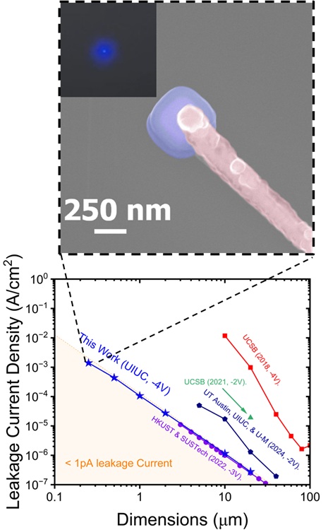
Picture: Top-down fabricated submicron LEDs (250nm dimensions) and (bottom) leakage current density benchmark with literature.
“The conventional sidewall passivation methods, which work well for micro-LEDs, are not sufficient when we push the dimensions into the submicron realm,” says Bayram, an Intel Alumni Endowed Faculty Scholar and director of the Innovative Compound semiconductoR LABoratory (ICORLAB). “The issue appears to be that, as the LED mesa size becomes comparable to the distance carriers can diffuse laterally, the impact of the sidewalls and any associated non-radiative recombination becomes overwhelmingly dominant, even with current state-of-the-art passivation.”
The research indicates that, at these ultrasmall scales, the proportion of the LED’s active region affected by sidewall defects significantly increases. While the team achieved good recovery of sidewall damage, evidenced by low leakage currents, the standard passivation (an atomic-layer-deposited bilayer of aluminium oxide and silicon dioxide) could not sufficiently suppress surface recombination in these submicron devices.
This study underscores a critical hurdle for the practical implementation of top-down fabricated submicron LEDs. While the successful fabrication of 250nm LEDs with good electricals is a promising starting point, overcoming the efficiency cliff is paramount. “These results call for a fundamental rethinking of how we manage sidewall effects in these tiny light emitters,” says Bayram. “Novel passivation strategies, potentially involving new materials or techniques to prevent lateral carrier diffusion, will be essential to unlock the full potential of submicron LEDs for future technologies.”
The work was performed in the Micro and Nanotechnology Laboratory and Frederick Seitz Materials Research Laboratory Central Research Facilities at UIUC, funded in part by the Advanced Research Projects Agency-Energy (ARPA-E), US Department of Energy, under award number DE-AR0001558.


