


News: Microelectronics
5 June 2025
Monolithic HEMT-micro-LED integration
Southern University of Science and Technology in China has reported progress in lowering the on-resistance of indium gallium nitride (InGaN) micro-LEDs monolithically integrated with aluminium gallium nitride (AlGaN)-barrier high-electron-mobility transistors (HEMTs) as current drivers [Ran Zhang et al, IEEE Electron Device Letters, published online 19 May 2025].
The researchers reduced resistance by increasing the contact area between the micro-LED and HEMT, along with reducing the tendency to add defects during the micro-LED overgrowth process. The team sees potential for low-power-consumption mobile devices such as augmented-reality (AR) glasses, smartwatches, etc.
The micro-LED materials were selectively overgrown using metal-organic vapor phase epitaxy (MOVPE) on AlGaN/GaN HEMT templates (Figure 1). Silicon dioxide (SiO2) was used as the mask to select the areas for the micro-LED stacks. The SiO2 was from plasma-enhanced chemical vapor deposition (PECVD), patterned using inductively coupled plasma etch stopping at the GaN cap of the template.
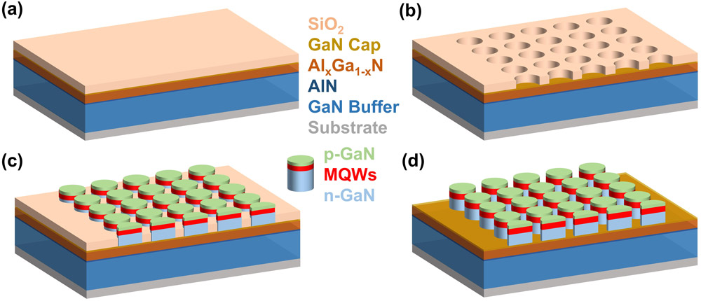
Figure 1: Monolithic integration scheme for selective area overgrowth: (a) 600nm SiO2 deposition on GaN HEMT template, (b) patterning SiO2 as overgrowth mask without etching HEMT material, (c) selective area overgrowth of micro-LEDs directly on HEMT surfaces, and (d) SiO2 mask removal.
The 40μm-diameter micro-LEDs consisted of up to 100nm heavily doped n++-GaN, 500nm n-GaN, 550nm InGaN/GaN multiple quantum wells (MQWs), and 150nm of p-GaN.
The researchers explain: “The regrown n-GaN functions simultaneously as the micro-LED cathode and HEMT drain. The n++-GaN layer facilitates a lower AlGaN band edge and effectively reduces the barrier height at the n-GaN/AlGaN interface.”
The SiO2 was removed by a buffered oxide etch solution before fabricating the HEMT transistor component (Figure 2). The source and drain for the HEMTs consisted of annealed titanium/aluminium/nickel/gold (Ti/Al/Ni/Au) stacks.
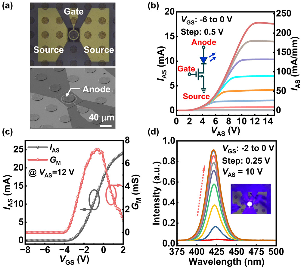
Figure 2: (a) Optical and scanning electron microscope images showing device layout, (b) output electrical characteristics, (c) transfer characteristics, and (d) electroluminescence of integrated HEMT−micro-LED devices.
Further Ni/Au was used for the p-contact of the LEDs and the HEMT gate. The p-contact consisted of metal layers that were so thin (7nm/7nm) that the contact was transparent and could be used as a current-spreading layer (CSL). The gate (20nm/100nm) formed a Schottky contact with the underlying AlGaN. The gate deposition step was also used to deposit the anode and cathode contact pads of the device.
The gate was 2x78.5μm wide (approximately the circumference of a 50μm-diameter circle), and 3μm long. The gate–source and gate–drain distances were 3 and 5μm, respectively. The HEMT delivered a maximum drain current density of 227mA/mm and a peak transconductance of 92mS/mm. The HEMT had a normally-on threshold of −4.1V. The on–off current ratio was 2.67x10⁵.
The micro-LED emission wavelength was around 423nm, with a blue-shift to shorter wavelengths as the current injection increased. The blue-shift was attributed to the quantum-confined Stark effect (QCSE) on the energy levels due to the changing electric field in the wells.
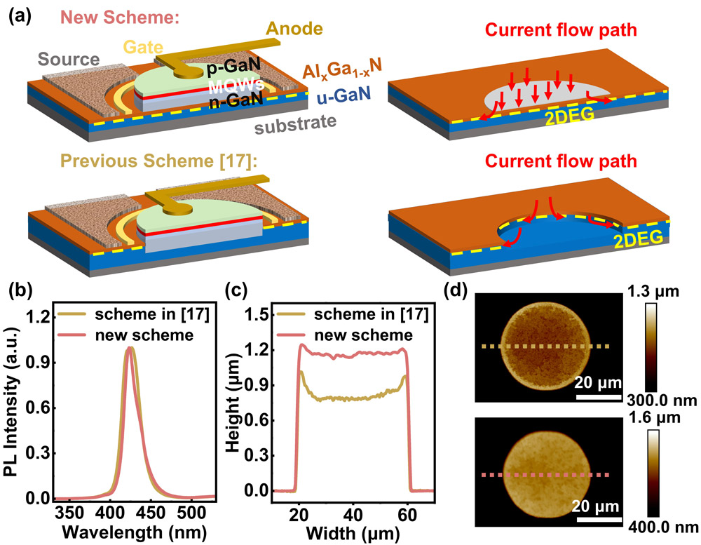
Figure 3: Comparison with previously reported integration scheme: (a) new and previous layout and current flow paths. (AlN insertion and GaN cap layers not shown for simplicity.) (b) Photoluminescence spectra, (c) surface profiles along line in (d), and (d) atomic force microscope (AFM) images of surface morphologies.
The researchers compared their latest devices with those using a structure that one of the team, Yufei Cai, helped develop at the University of Sheffield, UK (Figure 3). The main difference in the Sheffield structure was that the micro-LEDs were grown on the GaN buffer layer rather than the AlGaN HEMT barrier layer. To grow the micro-LEDs on the buffer it was necessary to etch 350nm down through the overlying materials and into the buffer, creating a damaged surface on which the micro-LED materials were grown. Avoiding this step reduces fabrication complexity and potential manufacturing cost.
The team comments: “Moreover, the current injection path in the new scheme encompasses the entire two-dimensional electron gas (2DEG) contact plane, namely the whole bottom area of n-GaN of the micro-LED. In contrast, current injection is restricted to the circular ring-shaped 2DEG region at the regrown LED-HEMT contact interface for the previous approach.”
The new fabrication scheme resulted in narrower photoluminescence peaks: 20.5nm compared with 24.8nm full-widths at half maximum (FWHM). The new and previous peak wavelengths were 423.2nm and 426.1nm, respectively. The researchers suggest that the narrower peaks could indicate smaller nonuniformity in both epi and quantum well thickness for the new scheme.
The researchers estimate from transmission-line model (TLM) measurements that the interface resistance between the n-GaN of the micro-LEDs and 2DEG of the HEMT channel was 0.68Ω-mm, compared with 4.8Ω-mm in the Sheffield scheme. Temperature-dependent measurements indicated that the thermionic emission was the dominant carrier transport mechanism between the 2DEG and micro-LED across the AlGaN barrier.
The researchers comment: “The thick space-charge region in the AlGaN barrier layer prevents direct tunneling, and carriers require thermal activation to overcome the interfacial potential barrier to inject into the 2DEG channel.”
The on-resistances at −2V gate potential were extracted at 80Ω-mm and 314Ω-mm for the new and old schemes, respectively. The researchers see further optimization opportunities in reducing the interface resistance further, along with improving the p-GaN deposition and recessing the source contact. The team suspects that avoiding etch damage to the overgrowth surface reduced the defectivity of the micro-LED epitaxial structure, reducing power-sapping current leakage paths.
Monolithic HEMT-micro-LED MOVPE PECVD InGaN AlGaN
https://doi.org/10.1109/led.2025.3571115
https://dx.doi.org/10.1021/acsaelm.0c00985
The author Mike Cooke is a freelance technology journalist who has worked in the semiconductor and advanced technology sectors since 1997.


