


News: Microelectronics
2 June 2025
Sumitomo Electric and Osaka Metropolitan fabricate GaN HEMT on 2-inch polycrystalline diamond
Japan’s Sumitomo Electric Industries Ltd (SEI) and Osaka Metropolitan University (OMU) have fabricated a gallium nitride high-electron mobility transistor (GaN HEMT) on a 2-inch polycrystalline diamond (PCD) substrate in a joint research project with the Japan Science and Technology Agency (JST). The technology is reckoned to be an important step toward achieving higher capacity and lower power consumption of core devices in mobile and satellite communications.
In recent years, as the volume of information in wireless communications has increased, there has been a demand for higher frequencies and higher output powers in high-frequency devices such as GaN HEMTs. However, the self-heating that occurs during operation limits the devices’ output power, resulting in signal transmission failures and other problems that reduce the performance and reliability of communications. To address these issues, OMU has improved the heat dissipation characteristics by using diamond (which has extremely high thermal conductivity) as a substrate for GaN HEMTs.
Generally, silicon and silicon carbide (SiC) are used as substrates for GaN HEMTs, but the thermal conductivity of diamond is about 12 times higher than that of silicon and 4–6 times higher than that of SiC. So, using diamond as a substrate can reduce thermal resistance by a quarter and half, respectively.
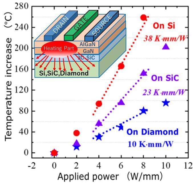
Picture: Comparison of heat dissipation of GaN HEMTs fabricated on silicon, SiC, and diamond (indicating that a smaller rise in temperature for the same applied power corresponds to better heat dissipation).
Previously, direct bonding to GaN layers without solder or bonding material was difficult due to the large grain size and poor surface roughness (5–6nm) of polycrystalline diamond. However, Sumitomo Electric has succeeded in directly bonding a GaN layer to a 2-inch polycrystalline diamond substrate by leveraging its diamond substrate polishing technology to reduce the surface roughness to halve the conventional level and by integrating OMU’s technology to transfer the GaN layer from the silicon substrate onto the polycrystalline diamond. Consequntly, the researchers have demonstrated GaN structure on polycrystalline diamond with uniform heat dissipation characteristics. The GaN layer used in this study was provided by Air Water Inc as a GaN/SiC epitaxial layer on a silicon substrate.
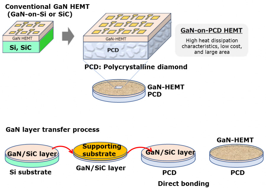
OMU contributed the technology for transferring GaN/SiC epitaxial layers grown on silicon substrates onto diamond substrates in order to fabricate the GaN HEMT devices. Sumitomo Electric contributed manufacturing and polishing technologies for large polycrystalline diamond substrates that have been used in heat dissipation materials and tool products such as heat sinks and bonding tools.
In the future, the researchers aim to develop the device performance and to optimize the bonding conditions using 4-inch substrates targeted at mass production, while accelerating the process.
The work is supported by Adaptable and Seamless Technology transfer Program through Target-driven R&D (A-STEP) from the Japan Science and Technology Agency (JST), Japan grant number JPMJTR222B.
GaN HEMTs on diamond demonstrates twice the heat dissipation of GaN-on-SiC
Sumitomo Electric develops N-polar GaN HEMT using Hf-based gate dielectric


