


News: Microelectronics
26 June 2025
AlYN-barrier GaN HEMTs for next generation devices
Cornell University in the USA and Germany’s Fraunhofer Institute for Applied Solid State Physics IAF have reported the use of aluminium yttrium nitride (AlYN) as a potential barrier material for gallium nitride (GaN) two-dimensional electron gas (2DEG) channel high-electron-mobility transistors (HEMTs) [Kazuki Nomoto, Appl. Phys. Lett., v126, p223509, 2025].
The team comments: “Using regrown n-GaN Ohmic contacts to the polarization-induced 2DEG, excellent HEMT DC performance with a low threshold voltage, a saturation drain current exceeding 400mA/mm, and a transconductance greater than 300mS/mm are obtained.”
The researchers also report “near-ideal sub-threshold swing minimum values of ~66–67mV/decade, highlighting excellent electrostatic gate control of the 2DEG channel conductivity due to a low interface trap density.”
The group sees such performance as potentially leading to high-efficiency, and high-frequency applications in next-generation wireless communication and power electronics systems.
Although yttrium does not fall in the traditional group III periodic table column sequence (boron (B), aluminium, gallium, indium,…), like them it has three electrons in the outermost shell. In fact, yttrium falls in the d-block of transition metals, and in modern period table terms is in group 3, while the traditional group III is put in group 13. Another group 3 elements is scandium (Sc), which also has seen implementation in research HEMTs in recent times. Lanthanum (La), the first f-block element (rare earths) also has three electrons in the outer shell, and has been subject to similar HEMT research exploration. The f-block elements do not have official group numbers.
In order to make an impact for future HEMTs these materials need to maintain high channel mobility, while improving breakdown and scaling characteristics. The breakdown voltage is related to the bandgap, so one needs larger bandgaps than that of present-day AlGaN-barrier devices. The Cornell, Fraunhofer and other groups have variously realized AlBN- and AlScN-barrier GaN HEMTs.
The epitaxial material structure (Figure 1) was grown by metal-organic chemical vapor deposition on 100mm-diameter semi-insulating (S.I.) 4H-polytype (0001) silicon carbide (SiC) substrate. The 9.7nm AlYN layer used solid tris(methylcyclopentadienyl)yttrium ((MCp)3Y), supplied by Dockweiler Chemicals, for the Y precursor.
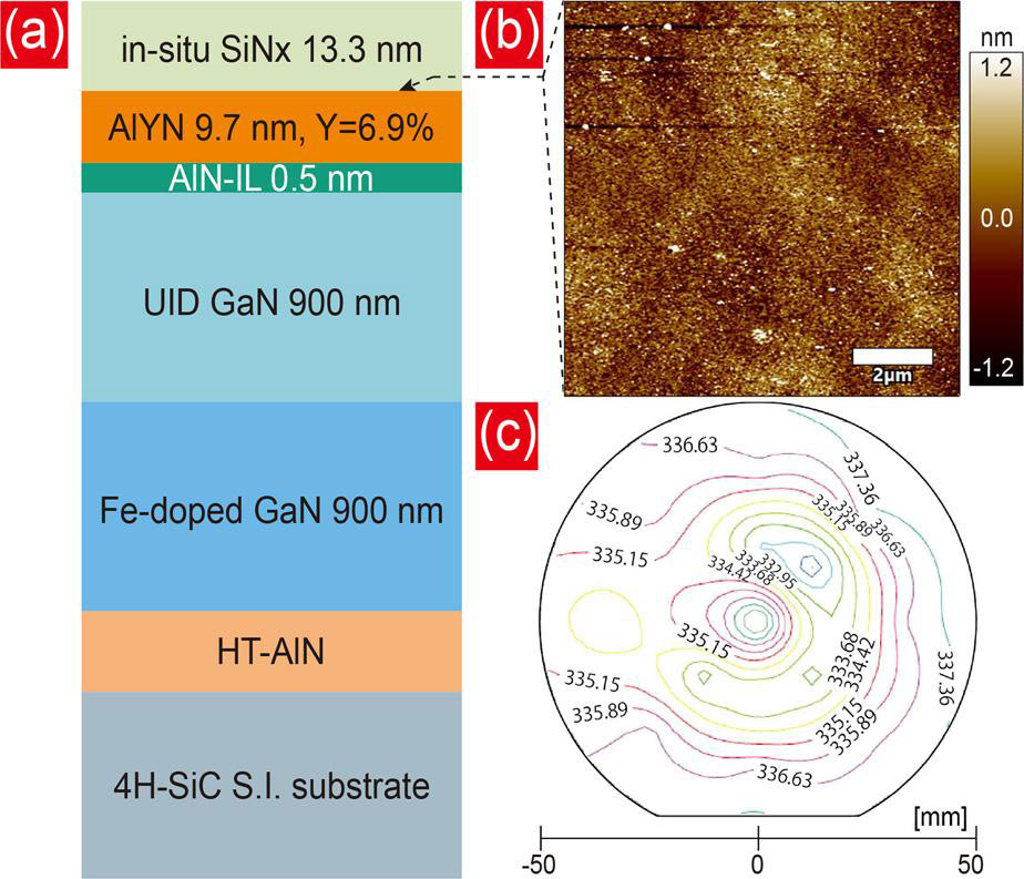
Figure 1: (a) Epitaxial AlYN/GaN MOCVD heterostructure. (b) Atomic force microscope (AFM) image of AlYN surface after removal of in situ silicon nitride (SiNx) by wet-etching. (c) Sheet resistance map across 100mm wafer.
The nucleation on the SiC was aluminium nitride (AlN) grown at high temperature (HT), followed by 900nm iron (Fe)-doped GaN lower buffer designed to compensate for residual donor impurities in the 900nm unintentionally doped (UID) upper buffer.
The AlYN barrier was grown on a thin AlN interlayer (IL) to improve barrier homogeneity. The epitaxial structure was completed by depositing SiNx for passivation of the AlYN surface. In particular the SiNx protected the Al-containing surface material from oxidation. AFM measurements over a 10μmxμm area with the SiNx removed showed a root mean square (RMS) surface roughness of 0.67nm. The sheet resistance was around 335Ω/□. The electron mobility in the two-dimensional electron gas (2DEG) that formed near the barrier/buffer interface was 1358cm2/V-s with electron density 1.37x10¹³/cm2.
The HEMTs (Figure 2) were fabricated with regrown source/drain n+-GaN contacts with titanium/gold (Ti/Au) metal electrodes. The gate and contact pads consisted of nickel/gold layers. The ~50nm-thick source/drain GaN regions were grown by molecular beam epitaxy (MBE).
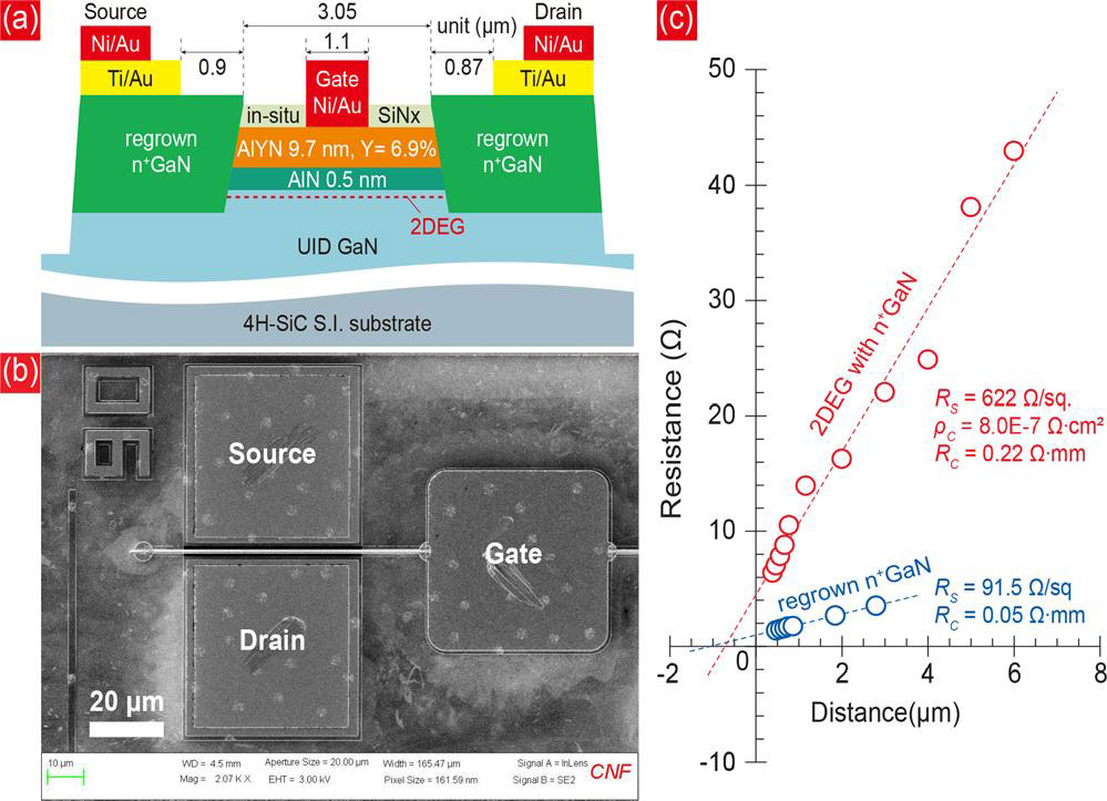
Figure 2: (a) Schematic cross section of HEMT. (b) Post-fabrication top-view scanning electron microscope (SEM) image. (c) Total resistance versus transmission line method (TLM) structure, showing contact and sheet resistances of regrown region and 2DEG channel.
The researchers believe that the rather high contact resistances from the metal/regrown GaN and regrown/2DEG GaN interfaces can be reduced in future work. Hall measurements probing the 2DEG with regrown Ohmic contacts gave 0.95x10¹³/cm2 carrier density, 1360cm2/V-s mobility, and 481Ω/□ sheet resistance. The reduction in carrier density, and associated increase in sheet resistance, were attributed to the source/drain regrowth. A control HEMT sample fabricated without regrown source/drain contacts showed no significant change in Hall properties from the values after MOCVD.
The researchers comment: “This suggests that the changes in sheet charge density are associated with specific steps involved in the regrowth process and post-regrowth treatments. The potential reasons could be due to the high temperature needed for regrowth and associated changes in strain in the barrier.”
Although the exact causes of the sheet resistance increase have not been determined as yet, the team was encouraged that the mobility was effectively unchanged.
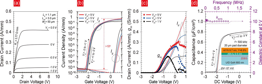
Figure 3: (a) Measured DC output. (b) Log scale and (c) linear scale transfer characteristics. (d) Measured capacitance–voltage (C–V) characteristics of AlYN/AlN/GaN-based metal-insulator-semiconductor (MIS) capacitor at 500kHz, and extracted dielectric constant across 10kHz–2MHz frequency range.
The fabricated AlYN-barrier HEMTs showed a maximum saturated drain current of 0.42A/mm at 0.5V gate potential (Figure 3). The on-resistance was 3.77Ω-mm. Gate voltage sweeps showed a drain-induced barrier lowering (DIBL) of around 9mV/V. The on/off current ratio was more than 109.
For negative gate potentials the gate current leakage was less than 1nA/mm, “indicating that the AlYN barrier layer is highly effective in restricting gate leakage current to allow effective gate modulation of the AlYN/GaN HEMT,” according to the team.
The threshold variation was −1.12V, −1.03V and −1.05V for drain biases of 1V, 5V and 9V, respectively. The peak extrinsic transconductance at 9V drain was 0.31S/mm. Capacitance measurements on MIS structures with 20μm-diameter nickel/gold pads showed relative dielectric constants of more than 10.
The researchers see their results as showing AlYN to be “an effective epitaxial gate dielectric with a decent relative dielectric constant that can simultaneously provide polarization-induced 2DEGs and appropriate insulating properties to serve as the gate barrier of AlYN/AlN/GaN HEMTs.”
In addition, the devices show subthreshold swings (SSs) down to just above 66mV/decade, near the room-temperature Boltzmann theoretical SS limit of 60mV/decade. In downward sweeps the lowest SS was 67.2mV/decade around 10−4A/mm, relatively independent of drain bias. For upward sweeps there was some dependence on bias, but slightly lower SS values were recorded around 66.5mV/decade for 1V bias.
The team comments: “These SS values indicate an interface trap density of Dit = 8x10¹¹/cm2-eV. The low SS values, even at high drain bias voltages, indicate that AlYN can serve as an attractive epitaxial barrier layer for the next generation of GaN HEMTs.”
https://doi.org/10.1063/5.0257333
The author Mike Cooke is a freelance technology journalist who has worked in the semiconductor and advanced technology sectors since 1997.


