


News: Microelectronics
17 July 2025
Elucidation of scattering mechanism of 2DEG in PAMBE-grown ScAlN/GaN heterostructure
As presented at the International Conference on Nitride Semiconductors (ICNS-15) in Malmö, Sweden (6–11 July) in a paper by Kouei Kubota et al, Japan’s Sumitomo Electric Industries Ltd — through joint research with the research group led by assistant professor Takuya Maeda of the University of Tokyo’s School of Engineering — has discovered the scattering mechanism of a two-dimensional electron gas (2DEG) in a heterojunction formed from scandium aluminium nitride (ScAlN) and gallium nitride (GaN). ScAlN/GaN is a strong candidate to be the barrier layer in next-generation high-frequency GaN high-electron-mobility transistors (GaN HEMTs).
In the GaN HEMT structures for high-frequency applications, GaN crystals are grown on a silicon carbide (SiC) substrate, and a heterojunction is formed by aluminium gallium nitride (AlGaN) grown by plasma-assisted molecular beam epitaxy (PAMBE) on top of the GaN crystal to create a two-dimensional electron gas (2DEG) on the interface, through which electrons move at high speed.
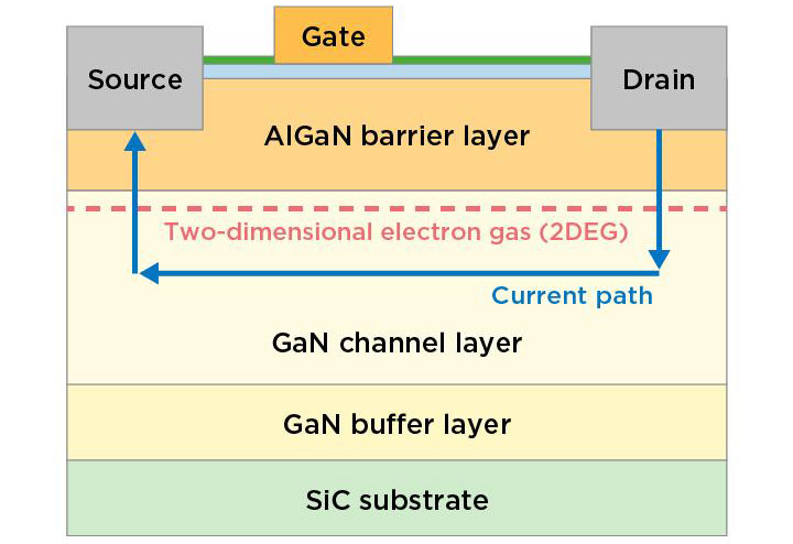
Picture: Structure of commonly used GaN HEMTs.
In the latest research work, Sumitomo Electric provided the high-quality GaN/SiC substrates. The University of Tokyo performed the fabrication of ScAlN/GaN heterojunctions on GaN/SiC substrates, as well as measurement and analysis. Specifically, transport properties were investigated in detail by temperature-dependent Hall-effect measurements.
ScAlN, which has a high electron generation capability, is attracting attention as a next-generation barrier layer to develop higher-frequency and higher-power GaN HEMTs. However, up to now the heterojunction between ScAlN and GaN attracts a high density of electrons but its mobility is limited by some scattering factors. The limiting factor for mobility has not been understood.
Due to the high density of the 2DEG, the research group pointed out the need to consider the increase in the electron effective mass caused by the non-parabolicity of the conduction band, and quantitatively discussed the impacts of polar optical phonon, acoustic deformation, and interface roughness scattering.
The new study found that the mobility of a 2DEG in a ScAlN/GaN heterostructure is limited mainly by interfacial roughness scattering (in which irregularities at the interface of a heterojunction impede the transfer of electrons), which is the dominant scattering mechanism.
Moving forward, the researchers therefore hope to improve the interfacial roughness and achieve high-density and high-mobility 2DEG formation to enhance the performance of GaN HEMTs used in next-generation high-frequency communications.
GaN HEMTs on diamond demonstrates twice the heat dissipation of GaN-on-SiC
Sumitomo Electric develops N-polar GaN HEMT using Hf-based gate dielectric


