


News: Microelectronics
17 July 2025
ScAlN ferroelectric AlGaN HEMT opportunities
University of Michigan, Ann Arbor, and Sandia National Laboratories in the USA have reported the use of scandium aluminium nitride (ScAlN) ferroelectric in aluminium gallium nitride (AlGaN) high-electron-mobility transistors (HEMTs) [Jiangnan Liu et al, Appl. Phys. Lett., v126, p253505, 2025]. The researchers see potential for next-generation non-volatile, reconfigurable power applications and high-temperature memory applications.
The incorporation of Al into the GaN channel material in HEMTs widens the bandgap, increasing the critical breakdown electric field and saturation carrier velocity. These features should enable efficient, high-gain power amplifiers, and high-temperature electronic applications, based on enhanced mm-wave and terahertz (THz) performance.
The breakdown field for Al0.5Ga0.5N is estimated at more than 10MV/cm, and the saturation velocity at more than 1.5x107cm/s, which could deliver power gain and density enhancements. Barriers to realizing these potentials include the typical offenders of poor ohmic contacts, lack of matching dielectric materials, and current collapse.
The III-nitride material for the HEMT (Figure 1) was grown by metal-organic chemical vapor deposition (MOCVD) on AlN/sapphire substrate, followed by molecular beam epitaxy (MBE) for the ScAlN. The MOCVD material also had a GaN cap to protect the Al-containing layers from oxidation during transfer to the MBE equipment. The material was heated to 800°C in the MBE system to remove the GaN cap before the ScAlN deposition.
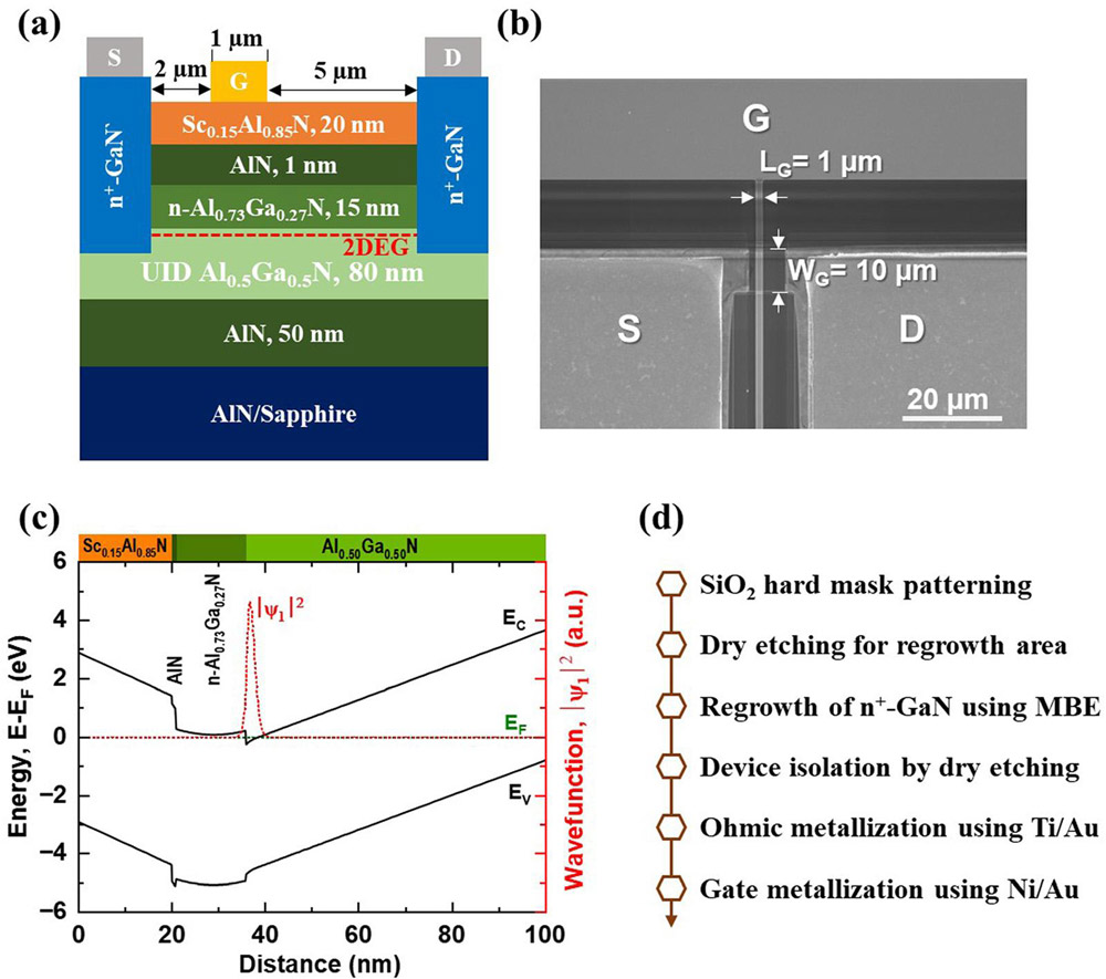
Figure 1: (a) ScAlN/AlGaN HEMT scheme and (b) top-view scanning electron microscope (SEM) image of device. (c) Energy-band diagram and ground-state wavefunction. Solid black curve, dotted green curve, and red dotted curve represent conduction- and valence-band energies, Fermi level, and wavefunction, respectively. (d) Fabrication process flow.
The structure enabled electron accumulation into a two-dimensional electron gas (2DEG) near the n-Al0.73Ga0.27N/Al0.5Ga0.5N interface. The material was metal-polar, including the ScAlN ferroelectric layer. The researchers calculate that the ScAlN enhanced the 2DEG electron carrier density from around 4.5x10¹²/cm2 for the III-nitride material without ScAlN to about 2x10¹³/cm2 with, due to strong polarization and large conduction-band discontinuity effects.
The HEMTs were fabricated with selective-area regrowth of n+-GaN source (S) and drain (D) contacts, using dry etch and MBE. The metal electrodes consisted of titanium/gold (Ti/Au) for the source and drain, and of nickel/gold for the Schottky gate (G). Although the S/D specific contact resistivity of 1.57mΩ-cm2 was relatively high, blamed on poor interface quality between regrown and epitaxial material structure, the team believes that “the reverse graded layer approach presents a promising method to further improve contact resistivity.”
The gate length (LG) was 1μm. The gate was asymmetrically placed with 2μm LGS and 5μm LGD. The gate width (WG) was 10μm.
The maximum drain current at 1V gate potential and 5V drain bias was 16.3mA/mm (Figure 2). The on/off current ratio was in the order of 106 between 1V and −25V, respectively. The gate leakage was 5.53nA/mm in the off-state. “This result indicates that the off-state current is limited by the gate current. The polarization-driven modulation enhances gate control and improves subthreshold swing (SS),” the researchers comment.
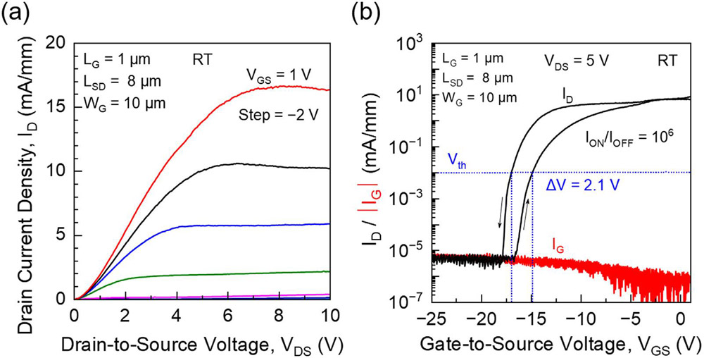
Figure 2: (a) Static characteristics of fabricated ScAlN/AlGaN HEMT at room temperature (RT). (b) Transfer curves (black curve) and gate leakage current (red curve), at 5V drain bias. Threshold voltage (Vth) defined at 0.01mA/mm. Vertical blue dotted lines indicate forward and backward Vth.
The current flow shows a counter-clockwise hysteresis loop. The Vth gap between the up- and downward VGS sweeps was 2.1V. The researchers say that this indicates that ScAlN/AlGaN HEMTs are promising candidates for next-generation memory applications. Reducing the drain bias to 1V increased the gap to 6.4V, due to a large Vth shift in the down-sweep.
The team reports: “An increase in off-state current, which corresponds to gate leakage current increase (IG = 1.93x10⁶mA/mm for VDS = 1 and 5.53x10⁶mA/mm for VDS = 5V) under high VDS bias, indicates that electrons are captured/trapped in the barrier layers. This trapping effect results in a positive shift in Vth when VGS is swept from positive to negative. It is noted that at lower drain bias voltages, the trapping/de-trapping effects have a reduced influence on the counterclockwise hysteresis, which is primarily governed by ferroelectric charge coupling.”
The measured subthreshold swing was lower during the down-sweeps: 65mV/decade and 104mV/decade for 1V and 5V drain biases, respectively. The corresponding values in the forward sweeps were 219V/decade and 333mV/decade.
The lower SS measured under backward gate-bias sweeps originated from electric field polarization in the ScAlN, facilitating the depletion of the 2DEG, according to the researchers, who add: “The tunable Vth and low SS exhibit great potential for future memory devices and multi-functional transistors.”
The threshold gap also increased with increasing ΔVGS step during the sweeps. The team explains: “This is because the backward scan leads to a sharp 2DEG depletion originating from the ScAlN switching and the smaller VGS step will increase the total poling time, reducing the hysteresis here.”
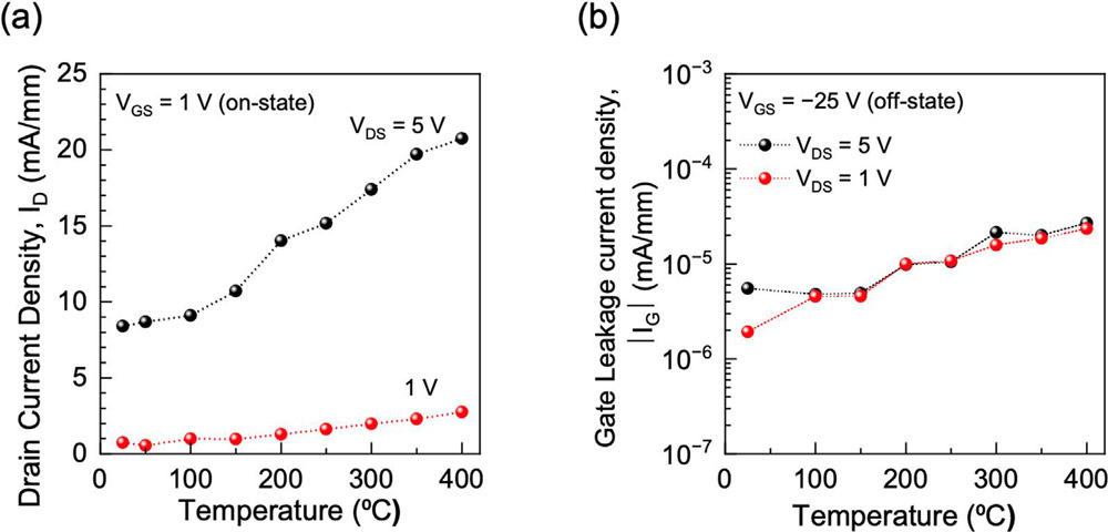
Figure 3: Variations in drain current (a) and gate leakage current (b) with temperature for different VDS.
The researchers also performed measurements at temperatures up to 400°C (Figure 3). The maximum drain current increased with temperature by 3.75x and 2.47x for 400°C over RT for drain biases of 1V and 5V, respectively. The increasing drain current suggests “thermally activated carrier transport at elevated temperatures, possibly due to thermionic emission over the n+-GaN/Al0.50Ga0.50N heterobarrier,” according to the researchers. Over the same temperature interval the gate leakage also increased by an order of magnitude (i.e. around 10x).
The team comments: “This increase in leakage current may be attributed to the thermal excitation of carriers and enhanced tunneling effects at higher temperatures. Despite this, the device maintains its functional integrity in the on-state, demonstrating its potential for high-temperature applications.”
ScAlN AlGaN HEMT GaN MOCVD MBE
https://doi.org/10.1063/5.0265601
The author Mike Cooke is a freelance technology journalist who has worked in the semiconductor and advanced technology sectors since 1997.


