


News: Microelectronics
24 July 2025
Gallium oxide HFET combines polytypes
Taiwan’s National Sun Yat-sen University claims the first demonstration of gallium oxide (Ga2O3) heterostructure field-effect transistors (HFETs) consisting of ε- on α-polymorph layers with tin (Sn)-doped transition between the two [Han-Yin Liu et al, IEEE Electron Device Letters published online 27 June 2025]. The heterostructure increased the off-state breakdown voltage (VBD) to 1725V, and reduced the specific on-resistance (Ron,sp) to 49.2mΩ-cm2, compared with a similar homostructure metal-semiconductor field-effect transistor (MESFET) consisting of just α-polytype material with Sn-doped channel (1239V breakdown, 260mΩ-cm2 specific on-resistance).
Ga2O3 is being intensively studied as a potential next-generation material for power electronics, based on its ultrawide bandgap and the associated expected higher critical breakdown field, relative to wide-bandgap semiconductors such as gallium nitride (GaN) and silicon carbide (SiC). Other potentials include deep-ultraviolet (DUV) optoelectronics, and radio-frequency (RF) electronics.
Most of this research is based on the stable β-polytype. The α and ε phases are metastable. The team comments that, among the various metastable polytypes, “ε-Ga2O3 is the second-most stable structure that exhibits ferroelectric characteristics with significant spontaneous polarization, surpassing III−nitrides, and enabling the formation of a high-density two-dimensional electron gas (2DEG) at heterojunctions without modulation doping.”
The researchers used mist chemical vapor deposition (mist-CVD) to apply the Ga2O3 polytype HFET layers to a 1cmx1cm c-plane sapphire substrate (Figure 1). The Ga precursor consisted of its acetylacetonate dissolved in deionized water. The Sn-doping precursor was tin (IV) chloride pentahydrate. The 150nm α-polytype layer was grown at 450°C, before the Sn doped and ε-polytype materials. A reference device was also fabricated from an all α-polytype structure grown on r-plane sapphire deposited at 600°C.
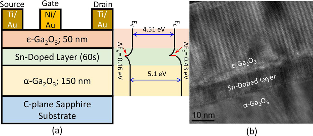
Figure 1: (a) ε-/α-Ga2O3 HFET structure and corresponding energy band diagram. (b) Transmission electron microscope (TEM) cross-sectional image.
The team comments: “The Sn-doped layer in the HFET serves dual functions: (1) providing high electron concentration to reduce the resistivity of the channel layer and (2) acting as a phase transition layer to promote the formation of ε-Ga2O3.”
Thermal evaporation was used to deposit metal electrodes for the HFETs: titanium/gold (Ti/Au) for the source and drain, nickel/gold (Ni/Au) for the 5µm-long Schottky-barrier gate. The gate width was 754µm. The gate was placed 10µm from the drain in the 20µm source−drain gap.
The effect of the Sn doping was expected to be an accumulation of electron (i.e. negative charge) carriers due to a conduction-band minimum there. The researchers add a caution: “Further experimental validation is required to confirm the detailed band alignment at the heterointerface.”
The crystal structures of the various layers were confirmed by x-ray diffraction analysis. While the Ga2O3 grown on c-plane sapphire showed an ε/α composition, the material on the r-plane substrate was all α. Study of the widths of the various peaks suggested that the material on c-plane sapphire was more crystalline. This was due mostly to a better lattice match between the bottom α layer with c-plane sapphire, relative to r-plane. The researchers note that the ε layer had even narrower x-ray peaks, suggesting that it had even better crystallinity than the α-Ga2O3.
The effect of more crystalline ε/α structure was seen in Hall-effect measurements: 2.91x10¹⁸/cm3 carrier density and 19.1cm2/V-s mobility, compared with 6.5x10¹⁷/cm3 and 51.42/V-s, respectively, for the all-α material.
The team comments: “The better crystallinity, fewer trapping centers, and conduction-band offset barrier make ε-Ga2O3/α-Ga2O3 exhibit higher electron density than α-Ga2O3 even with the same Sn doping concentration.”
Linear transmission-line model (TLM) measurements also showed lower Ti/Au contact and channel sheet resistances (Rsh) for the ε/α HFET: 4517Ω/□ sheet resistance, 11.63Ω-mm contact resistance, and 2.66x10⁻⁴Ω-cm2 specific contact resistivity, compared with 7428Ω/□, 46.35Ω-mm, and 4.62x10⁻³Ω-cm2, respectively, for the MESFET material.
Secondary-ion mass spectroscopy (SIMS) showed that the Sn-doped layer was thinner in the ε/α structure, 13.24nm, compared with 26.12nm in the all α material.
The researchers point out: “Normally, a wider Sn distribution range allows more Sn4+ ions to diffuse into the Ga2O3 epi-layer, replacing a greater number of Ga3+ ions with Sn4+. This substitution effectively reduces resistivity. However, contrary to this expectation, ε-Ga2O3/α-Ga2O3 demonstrates a lower Rsh and higher electron density compared to α-Ga2O3 as characterized in TLM and Hall-effect measurements. Previous research has predicted that polarization charges are induced at the ε-Ga2O3/α-Ga2O3 heterojunction. It is therefore presumed that these induced polarization charges increase the electron density, thereby reducing Rsh.”
The HFET showed much better performance for almost all the usual transistor characteristics (Table 1). The more negative threshold (Vt) might be seen as a drawback for the normally-off performance often desired in power systems. This threshold behavior is a natural result of the higher carrier concentration in the channel for the ε-Ga2O3/α-Ga2O3 HFET structure.
Table 1: On/off current ratio (ION/IOFF), threshold voltage (Vt), maximum transconductance (gm,max), gate leakage current (IG) at −10V gate potential, maximum drain current (ID) at 2V VGS and 30V VDS (300K and 450K), specific on-resistance (Ron,sp at 300K/450K), off-state (−18V gate) breakdown voltage (VBD), and power figure-of-merit (PFoM).
| Characteristic | α-Ga2O3 MESFET | ε-Ga2O3/α-Ga2O3 HFET |
| ION/IOFF | 1.4x10⁹ | 109 |
| Vt | −3.5V | −6.7V |
| gm,max | 1.63mS/mm | 8.67mS/mm |
| IG | 6.41x10⁻⁷mA/mm | 6.79×10⁻⁸mA/mm |
| ID @ 300K | 5.71mA/mm | 33.47mA/mm |
| ID @ 450K | 3.54mA/mm | 25.77mA/mm |
| Ron,sp @ 300K | 260mΩ-cm2 | 49.2mΩ-cm2 |
| Ron,sp @ 450K | 419mΩ-cm2 | 61mΩ-cm2 |
| VBD | 1239V | 1725V |
| PFoM | 5.9MW/cm2 | 60.48MW/cm2 |
The off-state leakage was dominated by current flow through the gate. The team comments that this may be due to “surface leakage paths caused by electrons hopping through the surface traps in the off-state,” adding: “The higher lattice mismatch between α-Ga2O3 and the r-plane sapphire substrate results in a higher density of surface traps, increasing surface leakage and IG.”
The HFET also demonstrated a smaller degradation in performance between room temperature (300K) and 450K. The researchers write: “The better thermal stability of ε-Ga2O3/α-Ga2O3 HFET is attributed to the conduction-band offset at the heterointerface, which acts as a barrier to confine electrons within the channel region, even at 450K.”
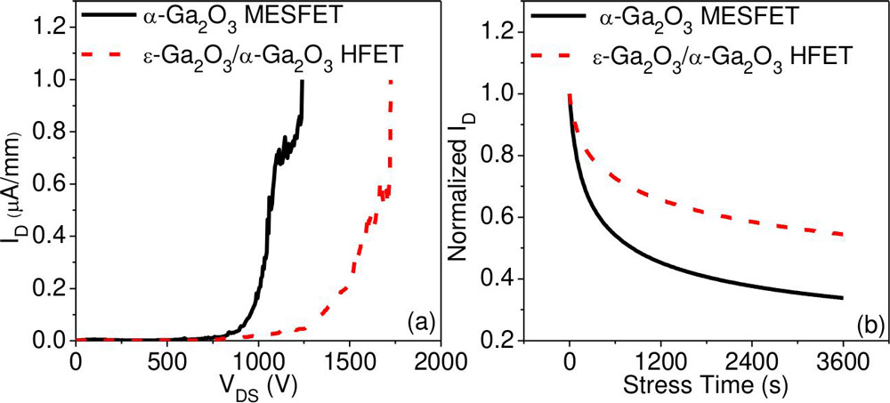
Figure 2: (a) Off-state breakdown voltage and (b) ID variation during drain stress test for α-Ga2O3 MESFET and ε-Ga2O3/α-Ga2O3 HFET with Sn-doped channel layers.
The higher off-state breakdown (Figure 2), and lower on-resistance lead to a high power figure-of-merit (VBD2/Ron,sp) of 60.48MW/cm2. The researchers comment: “The smaller Sn distribution range in ε-Ga2O3/α-Ga2O3 heterostructure shows that electrons are well-confined within a localized region, effectively suppressing leakage current and subsequently enhancing VBD.”
Drain bias stress testing was carried out at 0V VGS and 20V VDS. Over the 3600 seconds (also known as 1 hour) of the test, the drain current in the HFET degraded by 45.6%, compared with 66.2% for the homostructure MESFET. The team comments: “The relatively stable ID variation in the ε-Ga2O3/α-Ga2O3 HFET indicates that trapping effects are less significant compared to those in the α-Ga2O3 MESFET.”
Gallium oxide HFET Mist CVD MESFET
https://doi.org/10.1109/LED.2025.3584033
The author Mike Cooke is a freelance technology journalist who has worked in the semiconductor and advanced technology sectors since 1997.


