


News: Microelectronics
29 July 2025
Infineon launches CoolSiC MOSFETs 1200V G2 in Q-DPAK package
Infineon Technologies AG Munich, Germany has launched the CoolSiC MOSFETs 1200V G2 in a top-side-cooled (TSC) Q-DPAK package. Delivering what is said to be optimized thermal performance, system efficiency and power density, the new devices were specifically designed for demanding industrial applications that require high performance and reliability, such as electric vehicle chargers, solar inverters, uninterruptible power supplies, motor drives, and solid-state circuit breakers.
The new CoolSiC 1200V G2 technology offers significant improvements over the previous generation, enabling up to 25% lower switching losses for equivalent RDS(on) devices, increasing system efficiency by up to 0.1%. Utilizing Infineon’s improved .XT die attach interconnection technology, the G2 devices achieve more than 15% lower thermal resistance and an 11% reduction in MOSFET temperature compared with G1 family products. RDS(on) values ranging from 4mΩ to 78mΩ, along with a broad product portfolio, enable designers the flexibility to optimize system performance for their target applications. Furthermore, the new technology supports overload operation up to a junction temperature (Tvj) of 200°C and features high robustness against parasitic turn-on, ensuring reliable operation under dynamic and demanding conditions.
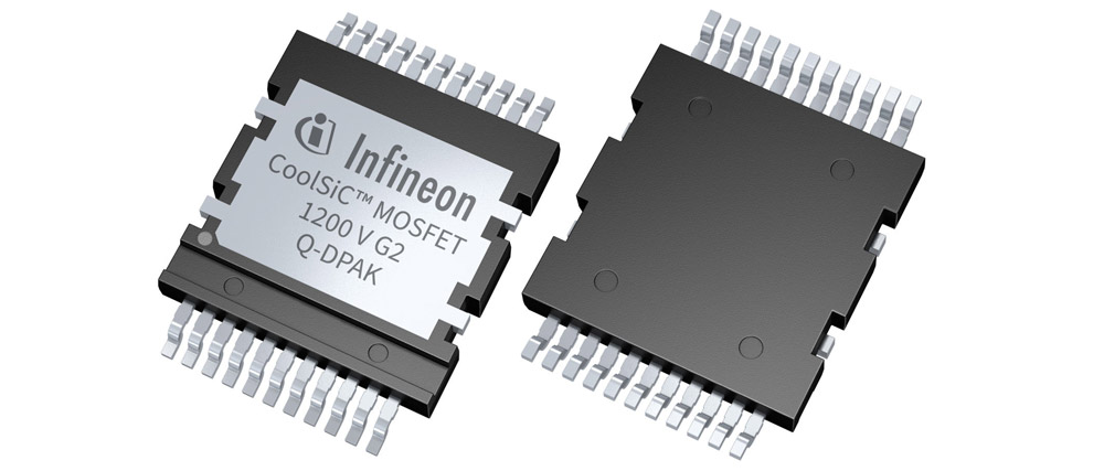
Picture: The CoolSiC MOSFETs 1200V G2 in a top-side-cooled Q-DPAK package.
The CoolSiC MOSFETs 1200V G2 are available in two Q-DPAK configurations: a single switch and a dual half-bridge. Both variants are part of Infineon’s broader X-DPAK top-side-cooling platform. With a standardized package height of 2.3mm across all TSC variants – including Q-DPAK and TOLT – the platform offers design flexibility and enables customers to scale and combine different products under a single heatsink assembly. This design flexibility simplifies advanced power system development, making it easier for customers to customize and scale their solutions.
The Q-DPAK package enhances thermal performance by enabling direct heat dissipation from the device’s top surface to the heatsink. This direct thermal path delivers significantly better heat transfer efficiency than traditional bottom-side-cooled packages, enabling more compact designs. Additionally, the Q-DPAK package layout design allows for minimized parasitic inductance, which is critical for higher switching speeds. This enhances system efficiency and reduces voltage overshoot risk. The small footprint of the package supports compact system designs, while its compatibility with automated assembly processes simplifies manufacturing, ensuring cost efficiency and scalability.
The CoolSiC MOSFET 1200V G2 in Q-DPAK single switch and dual half-bridge package variants are available now.
Infineon adds Q-DPAK and TOLL packages to industrial CoolSiC MOSFETs 650V G2 range
Infineon launches CoolSiC MOSFET Generation 2
Infineon makes available new-generation 1200V CoolSiC trench MOSFET in TO263-7 package


