


News: Microelectronics
2 July 2025
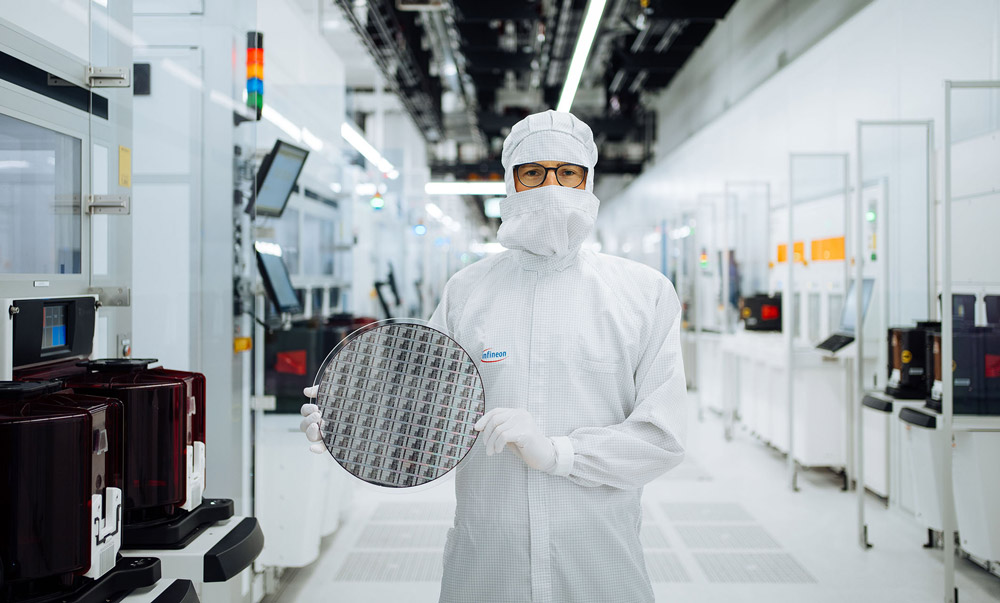
Infineon on track to ship customer samples of GaN on 300mm wafers in Q4/2025
Infineon Technologies AG of Munich, Germany says that its scalable gallium nitride (GaN) manufacturing on 300mm wafers is on track for first samples to be available to customers as of fourth-quarter 2025, positioning it to expand its customer base and reinforce its position as a leading integrated device manufacturer (IDM) in the GaN market as demand continues to grow. The GaN market for power applications will grow by 36% annually to about $2.5bn by 2030, forecasts Yole Group in its report ‘Power SiC and GaN Compound Semiconductor Market Monitor, Q1 2025’.
Infineon’s capabilities span all three relevant materials: silicon (Si), silicon carbide (SiC) and gallium nitride. With higher power density, faster switching speeds, and lower power losses, GaN enables smaller designs, reducing energy consumption and heat generation in electronic devices like smartphone chargers, industrial and humanoid robots or solar inverters.
“Our fully scaled-up 300mm GaN manufacturing will allow us to deliver highest value to our customers even faster while moving towards cost parity for comparable silicon and GaN products,” says Johannes Schoiswohl, head of Infineon’s GaN business line. “Almost a year after the announcement of Infineon’s breakthrough in 300mm GaN wafer technology, we are pleased that our transition process is well on track and that the industry has recognized the importance of Infineon’s GaN technology enabled by the strength of our IDM strategy.”
Infineon’s manufacturing strategy primarily relies on an IDM model — owning the entire semiconductor production process, from design to manufacturing and selling the final product. Its in-house manufacturing strategy is reckoned to be a key differentiator in the market, providing advantages such as high quality, faster time-to-market as well as superior design and development flexibility. Infineon has launched more than 40 new GaN products in the past year. Infineon says that it is committed to supporting its GaN customers and can scale capacity to meet their needs for reliable GaN power solutions.
Building on its technology, Infineon claims to have become the first semiconductor manufacturer to develop 300mm GaN power wafer technology within its existing high-volume manufacturing infrastructure. Chip production on 300mm wafers is technically more advanced and significantly more efficient compared with established 200mm wafers, as the larger wafer diameter allows 2.3 times more chips to be produced per wafer. These increased capabilities — combined with Infineon’s large team of GaN experts and the what is claimed to be industry’s broadest IP portfolio — are needed as GaN power semiconductors are being rapidly adopted in industrial, automotive, consumer and computing & communication applications, such as power supplies for AI systems, solar inverters, chargers and adapters or motor control systems.
Infineon pilots first 300mm power GaN wafer technology on existing large-scale 300mm silicon line
Infineon launches CoolGaN transistor families built on 8-inch foundry processes


