


News: Microelectronics
3 July 2025
Improving mobility in InAs quantum wells on GaAs substrate
Researchers in Germany have reported improved mobility in indium arsenide (InAs) quantum wells (QWs) on gallium arsenide (GaAs) substrates, particularly at cryogenic temperatures less than 120K, from a surface smoothing technique used during molecular beam epitaxy (MBE) [A. Aleksandrova et al, Appl. Phys. Lett., v126, p232109, 2025]. The team from Humboldt-Universität zu Berlin, Institut Kurz GmbH, and Paul-Drude-Institut für Festkörperelektronik, comment: “With the introduction of the surface smoothing, GaAs substrates thus replace InP substrates as a less-expensive and superior alternative.”
The researchers see their achievements as particularly interesting for quantum information processing. They explain: “Nanowires of InAs host Majorana zero modes, which are created by the strong spin–orbit coupling, in semiconductor–superconductor heterostructures. A pair of Majorana zero modes can realize a robust qubit for quantum computation that is immune to local perturbations. Thereby, the electronic coupling at the semiconductor–superconductor interface can be barrier-less since electrons are accumulated at the surface of InAs. In assembling a large number of qubits to build a quantum computer, defining narrow channels lithographically in heterostructures is far more practical than using epitaxially grown nanowires.”
Majorana zero modes refer to quantum theoretical quasi-particle constructs that are zero-energy, zero-charge quasi-particles with spin-1/2. In superconducting systems, these Majorana zero modes can arise as combinations of electrons and holes.
The team also suggests that their technique could benefit conventional electronic systems by boosting electron mobility in high-frequency wireless communication systems using InAs QW transistor structures.
The smoothing tackles lattice-matching problems that arise in InAs QW structures on GaAs, as opposed to indium phosphide (InP) or gallium antimonide (GaSb) substrates. The InAs mismatch with GaAs is 6.7%, compared with 3.1% and −0.6% for InP and GaSb, respectively. The buffer layer material between the substrate and QW undergoes plastic relaxation with such a large lattice mismatch, one effect of which is to present a cross-hatch pattern on the material surface.
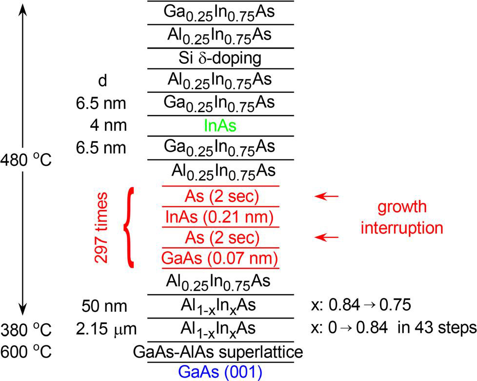
Figure 1: MBE growth sequence for InAs QW in AlInAs barriers. Red section shows growth interruption measures before Al0.25In0.75As layer for surface smoothing.
The MBE on GaAs began with a sequence of buffer layers (Figure 1). These consisted of a short-period superlattice grown at high temperature, and a sequence of AlInAs layers with graded indium composition in 50nm steps at low temperature. The final indium content in the buffer was 0.84.
The growth temperature was then increased to 480°C for the final layers, including the InAs QW. The first layer was AlInAs continuously graded down to 0.75 content in 50nm. The indium content overshoot in the buffer was designed to prevent further dislocations forming.
The team grew InAs QWs with and without surface smoothing measures. An insertion of 6.5nm GaInAs was used between the InAs QW and AlInAs barrier material. The researchers comment: “This insertion is crucial as Al-containing surfaces attract O2 molecules to be adsorbed. The resultant interface charges cause strong Coulomb scattering for the 2DEG in the QW if the InAs layer is not interfaced with the Ga0.25In0.75As layers.”
The surface smoothing measures consisted of a sequence of growth interruptions between GaAs and InAs layers to enhance adatom diffusion. The individual GaAs and InAs growth steps had target thicknesses of 0.25 and 0.75 atomic layers, respectively. The layers were thus equivalent to Ga0.25In0.75As.
A Si δ-doping layer was inserted in the upper barrier above the InAs QW. The position above the QW was varied.
Inspection with transmission electron microscopy (TEM) in bright-field (BF) and high-angle annular dark field (HAADF) modes showed that the threading dislocations were effectively trapped in the buffer layers with minimal penetration into the QW region. The team comments: “Even if the QWs were not entirely free of the threading dislocations, the dislocation density was too small to reduce the mobility of the 2DEGs.”
The surface smoothing was particularly effective in improving mobility at cryogenic temperatures (less than 120K) where the impact of phonon scattering is much reduced (Figure 2). The researchers point to previous work that showed that the mobility performance on GaAs substrate was comparable to that on more expensive InP.
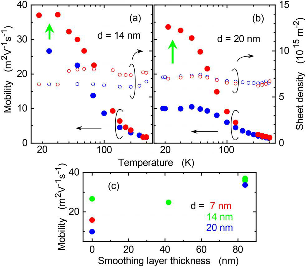
Figure 2: Improvement of electron mobility by introduction of smoothing layer. (a, b) Filled and open circles show respective mobility and sheet carrier concentration variations with temperature in InAs QW two-dimensional electron gas (2DEG). Red and blue circles correspond to QWs with and without the smoothing layer, respectively. Distance d of δ-doping from (Ga,In)As layer was 14nm in (a) and 20nm in (b). Green arrows indicate mobility increase enabled by surface smoothing. (c) Variation of mobility with thickness of smoothing layer.
A puzzling aspect was that the cross-hatch pattern associated with strain relaxation between the substrate and upper layers of the heterostructure continued to be apparent even with the surface smoothing process. The researchers comment: “It is emphasized that the surface smoothing does not change the cross-hatch morphology since the height modulation associated with it is much larger than what the enhancement of the surface migration by growth interruptions can smooth out.”
According to cross-sectional transmission electron microscope inspection (Figure 3), the surface smoothing reduces the effect of ‘step bunching’ introduced during the buffer growth. The team comments: “The surface smoothing must eliminate the steps whose height is increased to be much larger than the monoatomic-layer thickness by the step bunching.”
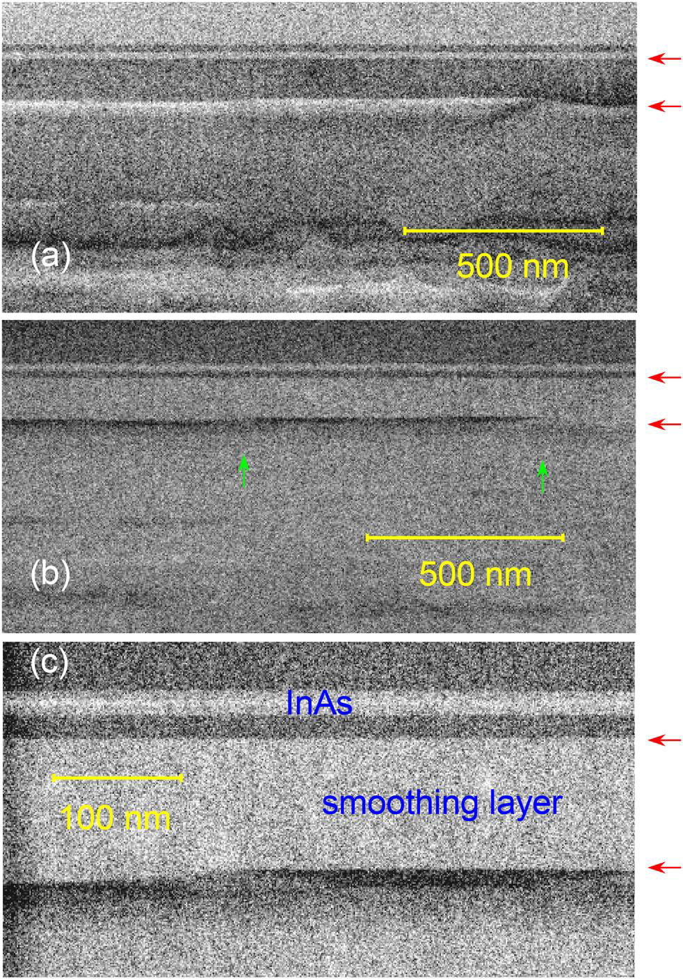
Figure 3: Removal of surface steps from smoothing. Transmission electron micrographs of QW region in BF (a) and HAADF (b) modes. (c) Magnified view of HAADF image. Red arrows point to top and bottom interfaces of smoothing layer. Green arrows show surface steps generated by bunching.
The step bunching occurred over distances significantly less than the carrier mean free path, creating opportunities for scattering and thus negatively impacting mobility. By contrast, the quasi-period of the cross-hatch surface was typically larger than the mean free path, and thus minimally impacted mobility.
The researchers comment: “Owing to the enhancement of the surface migration, the interfaces of the InAs QW became flat and abrupt when the smoothing layer was introduced. The interface scattering was consequently suppressed with improving the mobility, at least, to be as large as that obtained using InP substrates.”
The team also reports that they have attempted to use the surface smoothing technique on InP substrates, but the resulting InAs QWs showed no recognizable improvement of mobility. The researchers comment: “The interface scattering originating from the surface steps in the case of the InP substrates is hence suggested to be negligible compared to the impurity-limited mobility achievable with our MBE system.”
Another potential variation would be to use AlAs rather than GaAs in the smoothing sequence. However, this again failed — indeed, the surface became rougher and there was no mobility improvement.
The researchers comment: “The surface migration of the adatoms is indicated to be more difficult to enhance for AlAs than for GaAs. To be specific, AlAs may prefer to form islands, presumably due to a limited diffusion of the adatoms. The growth interruption would enlarge the island size instead of contributing to the step flow for the existing terraces.”
InAs quantum wells GaAs substrate InAs GaAs MBE
https://doi.org/10.1063/5.0268057
The author Mike Cooke is a freelance technology journalist who has worked in the semiconductor and advanced technology sectors since 1997.


