


News: Microelectronics
5 December 2025
X-FAB’s XbloX accelerates time-to-market for scalable, high-performance SiC MOSFETs
Through its XbloX platform, analog/mixed-signal and specialty foundry X-FAB says that it is offering easy access to a standardized yet flexible set of silicon carbide (SiC) process technologies that accelerate the development of advanced power devices. From rapid prototyping to full production, the modular and fully scalable XbloX platform helps SiC device developers to expedite engineering assessments and technology release, with production starts achieved up to nine months faster than traditional methods, it is reckoned.
Many next-generation SiC power metal-oxide-semiconductor field-effect transistors (MOSFETs) are currently up for design and development in sectors that include automotive, industrial, energy, and data center, making now the ideal time for fabless developers to engage with a foundry that can shorten time-to-market, the firm says.
The standardized and unique module configuration of the XbloX wide-bandgap (WBG) discrete foundry model offers two benefits for those designing or refining advanced SiC devices. Firstly, X-FAB takes on process development activities with the introduction of an innovative Process Installation Kit (PIK), where design and implant recipes provide the key differentiators. Secondly, the use of XbloX ensures that wafer manufacturing at X-FAB becomes a highly scalable activity in line with application requirements, differing considerably from the less scalable production provided by a traditional foundry model for customer-specific SiC technologies.
By taking advantage of the PIK and process blocks already developed at X-FAB, it becomes possible to reduce process development resources accordingly. Customers benefit from expedited onboarding, far fewer design risks, and significantly faster development time. The planning phase, for example, is up to six times shorter than that required by conventional approaches, it is reckoned. Those taking advantage of XbloX are said to gain a competitive edge, with design engineers able to create a diverse product portfolio while achieving production timelines up to nine months faster than conventional development pathways.
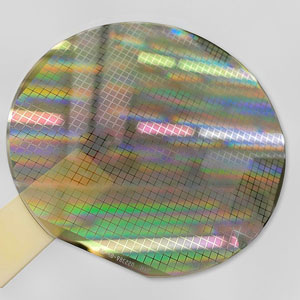 Picture: A silicon carbide wafer manufactured at X-FAB Texas.
“Thanks to a PIK, qualified SiC process development modules, and an automated onboarding process, customers need do little more than access our global hotline for support on block selection and deployment,” says Brian Throneberry, business director SiC Foundry at X-FAB. “We have robust rules in place to help guide design, mask tooling, engagement, and so on. Once the selection is finalized, XbloX automatically generates the process flow, which subsequently integrates quality systems, business functions, and commercial aspects for the customer. It’s a highly expedited way of providing customers with the flexibility required to build custom SiC MOSFET technologies at an accelerated rate.”
Scalable and streamlined, XbloX delivers simplified SiC process integration into CMOS-modeled process specifications, CMOS-modeled design rules, control plans, and FMEAs (failure mode and effects analysis). Customers using the platform can also benefit from any forthcoming X-FAB developments, such as new process modules.
Suitable for the smallest-form-factor planar SiC MOSFETs, the new, third-generation XbloX platform XSICM03 delivers considerably reduced cell pitch, enabling up to 30% more dies per wafer due to its improved on-state resistance.
X-FAB launches next-gen silicon carbide process platform for power MOSFET designs
Coherent, SkyWater and X-Fab all agree preliminary terms for US CHIPS Act funding
X-FAB and Soitec team to offer SmartSiC at Lubbock plant in Texas


