


News: LEDs
4 December 2025
Semi-polar epitaxial layer overgrowth improves micro-LED performance
University of California Santa Barbara in the USA reports on the potential of epitaxial layer overgrowth (ELO) to improve the efficiency and light output of micro-light-emitting diodes (μLEDs) [Stephen Gee et al, Semicond. Sci. Technol., v40, p115009, 2025].
The researchers comment: “Gallium nitride (GaN)-based micro-light-emitting diodes have emerged as a key technology enabling high-brightness, energy-efficient solutions for visible light communication, biosensing, and next-generation displays such as near-eye displays for virtual and augmented reality.”
ELO is a technique for reducing defects in the GaN material such as threading dislocations, which create leakage paths that sap energy efficiency. The researchers used the technique to create semi-polar material with reduced internal electric fields resulting from the charge polarization of the chemical bonds. The fields give rise to the quantum-confined Stark effect (QCSE), which can result in significant shifts in emission wavelength, something not wanted in displays.
The researchers chose semi-polar growth from the (20-21) plane as “particularly favorable for longer-wavelength emitters”. They add: “Its capability to support high-indium-content InGaN quantum wells with excellent crystal quality makes it especially promising for long-wavelength emission. The reduced polarization-related electric fields on this plane helps suppress the QCSE, especially at longer wavelengths where the QCSE is more pronounced, thereby enabling more stable emission wavelengths and lower efficiency droop.”
The researchers compared μLEDs fabricated from material grown on (20-21) ELO and (20-21) planar freestanding GaN (Figure 1). “Lateral growth stops the vertical propagation of threading dislocations (TDs) and reduces the TDD, improving device performance,” the researchers comment.
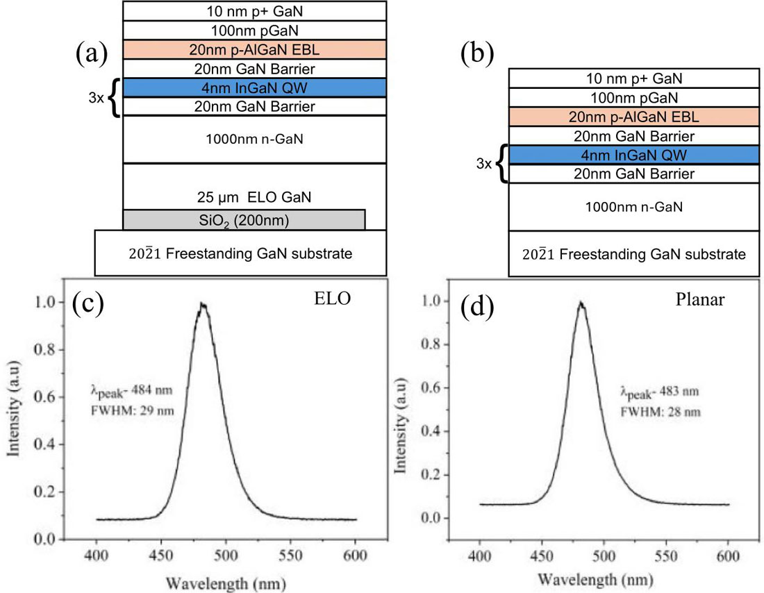
Figure 1: Schematic diagrams of (a) ELO and (b) planar μLED epitaxial structures with corresponding emission spectra for (c) ELO and (d) planar μLEDs.
The ELO material was grown out of 5μm-wide windows in a 200nm-thick plasma-enhanced chemical vapor deposition (PECVD) silicon dioxide (SiO2) mask layer. The spacing between the windows was 55μm. Metal-organic chemical vapor deposition (MOCVD) was used for the ELO.
The first 400 minute ELO growth step resulted in GaN bars that were 25μm high and 40μm wide. The SiO2 mask was then removed using hydrofluoric acid with the aim of improving uniformity and surface quality for the MOCVD device layers.
The electroluminescence (EL) spectra of the ELO had a peak at 484nm, close to the 483nm of the device on planar GaN.
The team comments: “This small wavelength shift observed in the ELO sample is attributed to its increased layer thickness and higher thermal impedance due to the air gap formed beneath the ELO GaN bars during the HF etching.”
μLEDs were fabricated with an indium tin oxide (ITO) current-spreading layer on the p-GaN. Sputtered SiO2 was deposited as a 300nm isolation layer. The metal electrodes consisted of titanium/gold on the p-side, titanium/aluminium/nickel/gold on the n-side.
The researchers report increased light output from the ELO devices relative to the μLEDs fabricated on planar material (Table 1). The improved performance was attributed to reduced threading dislocation density in the ELO, which decreases leakage and non-radiative recombination, such as through the Shockley-Read-Hall (SRH) mechanism.
Table 1: Comparison of measured light output for square μLEDs.
Device type |
Size | Injection current density | Measured light output |
| ELO | 10µm | 1x10³A/cm2 | 1.27µW |
| Planar | 10µm | 1x10³A/cm2 | 1.10µW |
| ELO | 10µm | 2x10³A/cm2 | 2.4µW |
| Planar | 10µm | 2x10³A/cm2 | 2.26µW |
| ELO | 15µm | 1x10³A/cm2 | 3.0µW |
| Planar | 15µm | 1x10³A/cm2 | 2.6µW |
| ELO | 15µm | 2x10³A/cm2 | 5.5µW |
| Planar | 15µm | 2x10³A/cm2 | 5.1µW |
The light output was measured from a calibrated silicon detector. The team comments: “While on-chip measurements suffer optical losses due to limited light collection, surface absorption, and limited light extraction, they provide consistent comparisons between devices.”
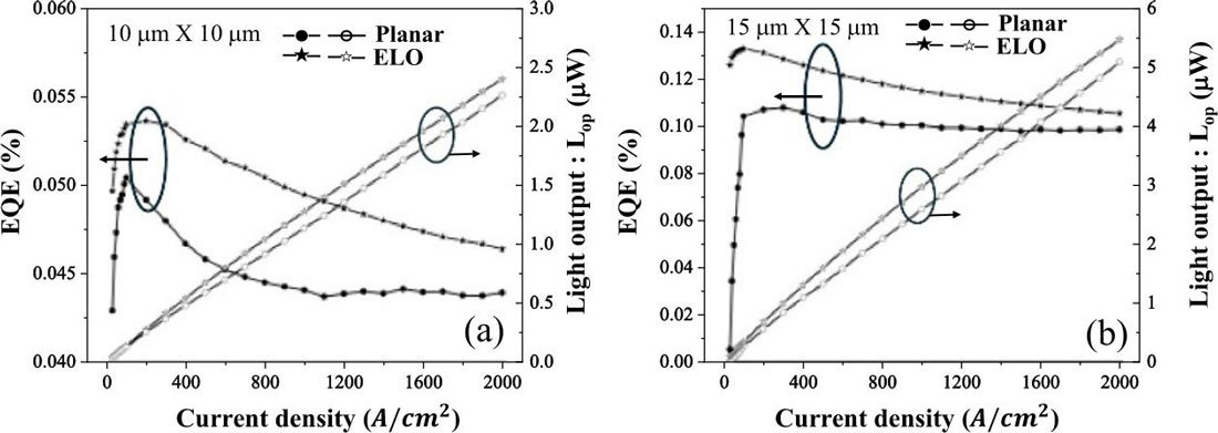
Figure 2: Dependence of EQE on current density for (a) 10μm and (b) 15μm-square ELO and planar μLEDs.
The measurement setup also resulted in very low EQE measurements for similar reasons (Figure 2). For what it is worth, the peak EQE of the 10μm-square LEDs were 0.051% and 0.054% for the planar and ELO devices, respectively. The ELO peak came at 200A/cm2, compared with 100A/cm2 for the planar LEDs. The larger 15μm LEDs achieved higher EQEs: 0.11% at 300A/cm2 for the planar device, and 0.13%, 100A/cm2 for ELO.
The researchers comment: “The change in EQE with LED size was likely due to the increased SRH recombination at the sidewall of the devices. We expect to get greatly improved EQE and light output power measurements with an improved device, encapsulation, and measurement in an integrating sphere to capture all emitted light.”
The wavelength (blue-)shift was smaller in the ELO device: 3nm at 2kA/cm2, compared with 6nm for the planar μLED.
The researchers conclude: “Future studies will implement improved sidewall treatments to reduce SRH recombination and further isolate the effects of lowered defect density. The combination of these improvements with previously reported liftoff techniques could allow for the development of highly efficiency semi-polar μLED displays.”
Semi-polar epitaxial layer overgrowth ELO Micro-LED MOCVD GaN
https://doi.org/10.1088/1361-6641/ae1bc9
The author Mike Cooke is a freelance technology journalist who has worked in the semiconductor and advanced technology sectors since 1997.


