


News: Microelectronics
18 December 2025
Quasi-vertical selective area growth GaN diode on silicon
Researchers based in France, USA and Italy claim the first demonstration of avalanche breakdown behavior in quasi-vertical gallium nitride (GaN) diodes fabricated from selective area growth (SAG) material on silicon (Si) substrate [Mohammed El Amrani et al, J. Appl. Phys., v138, p215701, 2025]. The advantage of avalanche breakdown is that it is non-destructive. The breakdown of the diodes was 720V at room temperature.
The team, from Université Grenoble Alpes in France, Stanford University in the USA, and University of Padova in Italy, believes that the performance of the devices can be improved “through the optimization of the design geometry and the implementation of an effective edge termination scheme.”
GaN enables high-voltage devices through the material’s wide bandgap, high electron mobility, and high electric field breakdown strength. Standard lateral device structures limit current and voltage handling to the low to medium range. Vertical devices should enable current to flow through a larger-area cross section, as opposed to the thin two-dimensional electron gas (2DEG) channel of lateral device structures.
Vertical device structures are typically fabricated from material grown on freestanding or native GaN substrates. This inhibits commercialization due to the high cost and small size of such wafers. The researchers comment: “GaN-on-silicon (GaN-on-Si) technology presents a promising alternative by combining the performance of GaN with the cost-effectiveness and mature infrastructure of large-diameter silicon wafers.”
Growth of GaN-on-Si suffers from lower material quality due to the large lattice mismatch and thermal expansion mismatch between the respective materials. SAG is a popular method for enhancing the quality of III-nitride heteroepitaxy on substrates such as silicon, sapphire, etc. SAG on Si has the added potential for integration between GaN power and silicon mainstream electronics.
The team comments: “Our results highlight the potential of SAG as a scalable platform for high-performance, avalanche-capable GaN power devices, bridging the gap between lateral GaN-on-silicon HEMTs and truly vertical GaN technologies.”
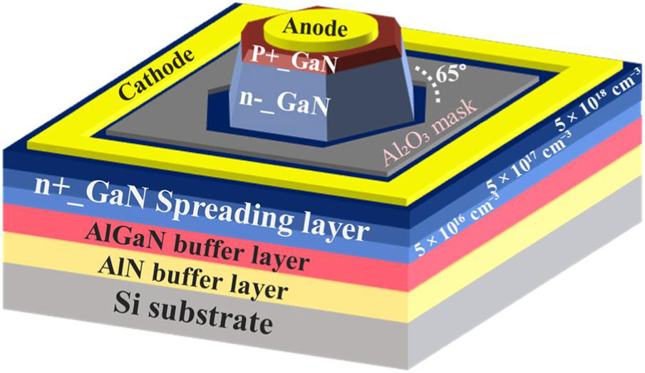
Figure 1: Schematic 3D cross section of quasi-vertical p–n diode.
The SAG was performed on a substrate with AlGaN/AlN buffer layers and three n+-type GaN current-spreading layers with increased doping (Figure 1). The SAG used a 50nm atomic layer deposition (ALD) aluminium oxide (Al2O3) hard mask. The SAG device structure consisted of a 8μm n--GaN drift layer, and a 0.8μm p-GaN anode. The growth resulted in 100μm-diameter hexagonal device mesas with around 65° bevel angle.
The researchers comment: “This unintentionally formed bevel serves a critical function in mitigating electric field crowding at the p–n junction edges. By providing a gradual transition at the mesa sidewalls, it helps reduce peak electric fields that typically lead to premature breakdown.”
Using the natural bevel as part of the fabrication strategy for directing the electric field away from the edges avoids the etch damage that normally arises when crafting device mesas. However, the researchers have found that additional peripheral protection is desirable for such diodes. The researchers estimated the dislocation density in the SAG material to be in the range 1–3x10⁸/cm2.
The magnesium-doped p-type layer of the diode was activated by thermal annealing at 800°C for 3 minutes. The researchers also applied a second thermal anneal at 700°C for 10 minutes in an effort “to improve the GaN crystal structure and further stabilize the activated Mg”. The 40μm-diameter anode metal contact consisted of nickel/gold; the cathode was formed by opening a window in the Al2O3 mask for the titanium/aluminium/nickel/gold electrode.
Capacitance–voltage measurements indicated a net doping concentration in the n−-drift layer of 1.6x10¹⁶/cm3.
The team reports: “The device achieves a current density of 1.4kA/cm2 at 10V and a specific on-resistance (Ron,sp) of 3.3mΩ-cm2 (determined from the slope of the V–J curve). Additionally, the diode exhibits a favorable turn-on voltage of 3V, measured at a current density of 1A/cm2, along with a high on/off current ratio of 1010.”
The ideality was non-ideal at around 3, indicating that the dominant recombination was through defects via the Shockley–Read–Hall mechanism. The high Ron,sp was mainly attributed to the quasi-vertical structure with an approximate 300μm lateral current conduction path between anode and cathode. A fully vertical device would reduce this to just the thickness of the layers.
Under reverse bias, the device underwent non-destructive breakdown at −720V at 298K (Figure 2). The devices were protected with Fluorinert to prevent arcing in air. The researchers attribute the “robust” breakdown performance in part to the avoidance of mesa etching in the SAG diode fabrication.
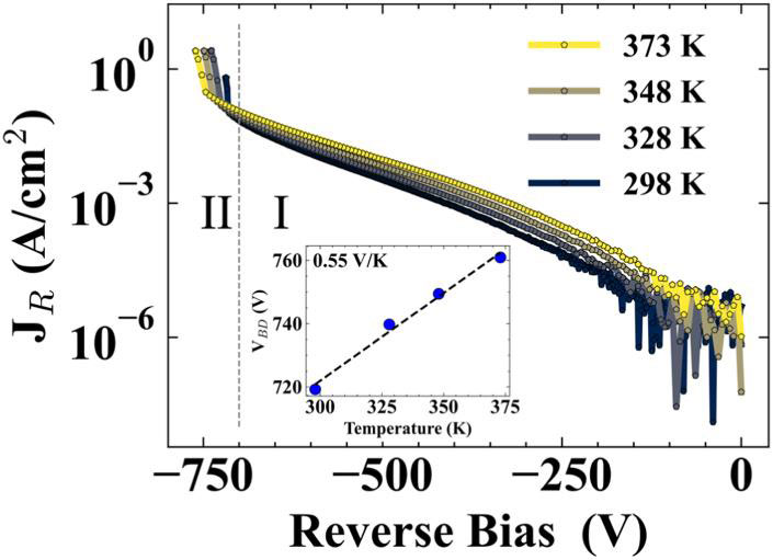
Figure 2: Typical temperature-dependent reverse current density–voltage (J–V) log-scale characteristics. Inset: extracted breakdown voltage as function of temperature.
The team reports: “The fabricated devices achieve up to ~75% of the theoretical parallel-plane breakdown voltage and ~91% of the Technology Computer-Aided Design (TCAD) Sentaurus Synopsys-simulated value, using the same bevel angle and doping profile, underscoring the effectiveness of the SAG approach.”
The behavior beyond –700V showed a rapid current increase, suggesting that the electric field was large enough for carrier multiplication through impact ionization, initiating avalanche breakdown. The researchers comment: “The observed positive temperature dependence of the breakdown voltage further confirms avalanche breakdown behavior—a hallmark of impact ionization.”
The researchers used Stanford’s unclamped inductive switching (UIS) test set up to evaluate the diode’s capability for withstanding transient voltage overshoot events. Energy stored in an inductor was applied to the diode by switching off a 1.7kV-rated silicon carbide transistor. The stress duration was 2.5μs.
The researchers comment: “The device under test (DUT) successfully endured over 3000 UIS pulses at a repetition rate of 1kHz before failure. During these cycles, the DUT consistently reached a voltage of approximately 800V, exceeding its static avalanche breakdown voltage of 720V, along with a peak current of 150mA.”
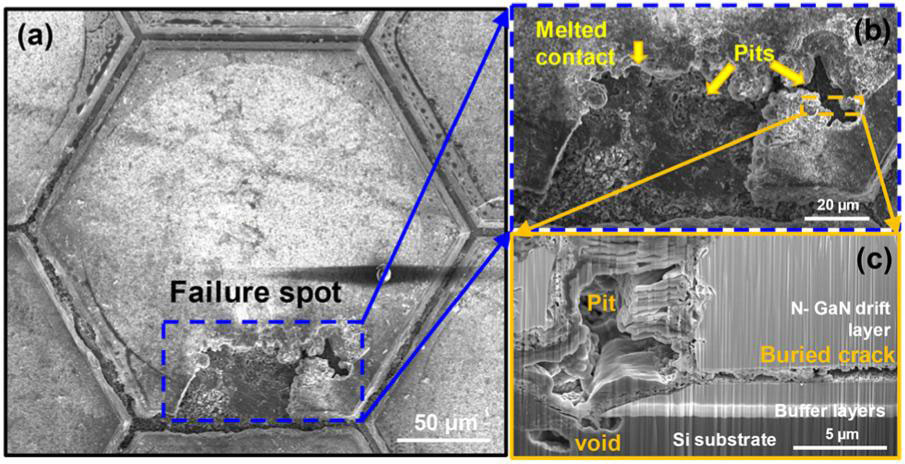
Figure 3: Post-failure scanning electron microscope (SEM) analysis of GaN diode: (a) top-view image showing surface damage; (b) magnified focused ion-beam (FIB)-SEM image near the anode edge; (c) cross-sectional FIB-SEM image revealing damage through n-GaN drift layer and underlying structure.
Destructive breakdown occurred when the UIS duration increased to 30μs (Figure 3). The team comments on experiments where light from the device was collected by a CCD detector: “When the stored energy in the inductor exceeds the diode’s safe operational limit — achieved by extending the gate-pulse duration — a sudden, bright flash appears as a narrow filament at the anode mesa edge. This localized glow marks the onset of destructive breakdown: the intense electric field concentrates at the mesa perimeter, initiating a high-current-density path that heats the material rapidly.”
The researchers add: “Due to the absence of dedicated edge termination structures in the diode mesa, the device underwent catastrophic structural failure likely driven by high localized current densities and intensified electric fields at the anode edge, exacerbating thermal stress and, thus, significant thermoelastic strain within the contact metal and GaN layer, consequently promoting crack initiation and pit formation. Implementing an effective edge termination structure is expected to mitigate localized electric field peaks, thereby enhancing the diode’s avalanche and surge voltage robustness.”
GaN diode GaN GaN-on-Si Silicon substrates
https://doi.org/10.1063/5.0299842
The author Mike Cooke is a freelance technology journalist who has worked in the semiconductor and advanced technology sectors since 1997.


