


News: Markets
29 December 2025
Co-packaged optics market to grow at 37% CAGR to $20bn by 2036
In its new report ‘Co-Packaged Optics (CPO) 2026-2036: Technologies, Market, and Forecasts’ by principal technology analyst Dr Yu-Han Chang, market research firm IDTechEx notes that, in recent years, optical transceiver technology has been steadily shifting toward placing the optics closer to the ASIC. Traditionally, pluggable modules inserted into the front panel of a switch sit at the edge of the printed circuit board and have long served as the standard solution for connecting switches and servers in data centers. They remain popular for their flexibility, ease of replacement, and straightforward scaling. However, they face growing challenges, especially rising power consumption and limits on how much bandwidth can be delivered per unit of front-panel area.
To address these constraints, the industry has begun migrating the optical engine closer to the switch ASIC in an effort to shorten the copper trace used for electrical signalling. Although these near-packaged approaches improve electrical performance, they still diverge from the well-established pluggable ecosystem, and key limitations remain. As a result, many in the industry expect the transition to progress directly toward fully integrated solutions such as co-packaged optics.
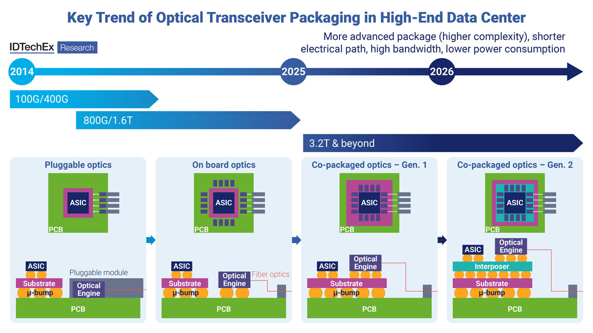
Picture: Key trends of optical transceivers in high-end data centers. Source: IDTechEx.
Importance of advanced packaging technologies for co-packaged optics
Traditional pluggable optical modules are increasingly constrained by signal loss, power consumption and latency because they require long electrical traces between the switch ASIC and the optical engine. Co-packaged optics overcomes these limitations by placing the optical engine much closer to the switching silicon. Its success depends on advanced semiconductor packaging technologies that enable high-density integration of photonic and electronic ICs, along with the seamless attachment of optical engines to switch ASICs or XPUs. This requires a range of packaging approaches, including 2.5D interposers, through-silicon vias (TSVs), fan-out wafer-level packaging (FO-WLP) and, more recently, 3D integration supported by hybrid bonding.
At its GPU Technology Conference (GTC 2025), NVIDIA introduced two new networking switch platforms, Spectrum X Photonics and Quantum X Photonics, both built on co packaged optics. Central to these platforms is TSMC’s System on Integrated Chips technology, which provides the 3D integration infrastructure for NVIDIA’s design. The SoIC X variant, TSMC’s advanced bumpless hybrid bonding process, enables vertical stacking of logic dies and other heterogeneous components at sub-ten-micron pitch. This dramatically shortens interconnect length and reduces resistance and latency.
Other major players, including Broadcom, have also adopted TSMC’s COUPE platform, underscoring the growing importance of 3D integration and hybrid bonding in CPO.
Co-packaged optics market trajectory
IDTechEx forecasts that the co-packaged optics market will rise at a robust compound annual growth rate (CAGR) of 37% from 2026 to more than $20bn by 2036. CPO network switches are expected to dominate revenue generation, driven by each switch potentially incorporating up to 16 CPO photonic integrated circuits (PICs). Optical interconnects for AI systems will constitute about 10% of the market, with each AI accelerator typically utilizing one optical interconnect PIC to meet increasing demands for high-speed data processing and communication in advanced computing applications.


