


News: Optoelectronics
1 December 2025
Avicena’s LightBundle optical links operating at 4Gbps per lane with transmitter current as low as 100µA per LED
At SuperCompute 2025 (SC25) in St Louis, MO, USA (16–21 November), Avicena Tech Corp of Sunnyvale, CA, USA has announced that its LightBundle micro-LED-based optical links now operate at 4Gbps per lane with transmitter currents as low as 100µA per LED. At this current, each link closes at a raw bit-error rate (BER) of 1x10–12 with an equivalent energy of 80fJ/bit per LED, all without forward error correction (FEC).
The firm says that this achievement highlights the LightBundle platform’s ability to deliver the world’s lowest-power optical interconnects for next-generation AI infrastructure by addressing the increasing bandwidth, distance and reliability requirements most efficiently.
Unlike laser-based optical engines — which cannot operate below a lasing threshold — micro-LEDs can scale transmit power to nearly arbitrarily low levels, limited primarily by the receiver’s signal-to-noise ratio. While silicon photonics can achieve low effective power by splitting a single external laser across many resonant modulators, micro-LEDs inherently generate their own light, dramatically simplifying packaging. Avicena’s micro-LED transmitters are only a few microns in size, require no temperature stabilization, and avoid complex control loops. These microscopic emitters can be arrayed at extremely high density to deliver terabits of aggregate bandwidth.
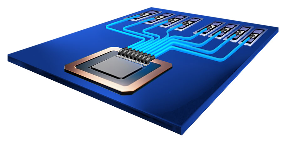
Picture: Scalable LightBundle chiplet platform for memory disaggregation.
Avicena says that this new power-per-lane milestone was enabled by its latest high-sensitivity receiver technology, developed in collaboration with manufacturing partners and incorporating optimized photodetectors derived from high-volume image-sensor processes.
Instead of serializing low-speed on-chip data (typically around 2Gb/s per lane) to very high-speed optical lanes, LightBundle transmits raw parallel data directly, dramatically simplifying integrated circuit (IC) input/output (I/O) architectures. This approach enables massive arrays of micro-LEDs to deliver unprecedented aggregate bandwidth at very low latency, low power consumption, while being easily integrated with any silicon node. LightBundle chiplet transceivers are well suited to various packaging architectures including co-packaged optics (CPO), on-board optics (OBO), pluggable optical modules, and wide memory interconnects.
“We already demonstrated an efficient micro-LED link in a live demo at ECOC 2025 in September. By further optimizing our highly sensitive receivers, we have managed to further reduce the operating currents of the micro-LEDs and obtained Tx energy consumption down further to tens of femtojoules for this part of the link,” says chief scientist Rob Kalman. “Combined with the unique properties of microLEDs, we can achieve unmatched energy efficiency in our LightBundle interconnects,” he adds. “This benchmark shows the scalability of our roadmap, how micro-LED technology can replace legacy laser-based links with a simpler, more reliable and far lower-power solution.”
This latest development builds on the ongoing work between Avicena and its hyperscale data-center, AI accelerator and memory partners to enable scale-up AI cluster architectures that span multiple racks and thousands of GPUs, dramatically increasing compute performance for emerging agentic AI workloads.
Avicena partners with ams OSRAM on production of ultra-low-energy chip-to-chip optical interconnects
Avicena demos optical link operating at record temperature of 235°C
Avicena acquires GaN micro-LED fab and engineering team from Nanosys


