


News: Microelectronics
28 August 2025
E-mode GaN HEMT breakdown beyond 10kV
Researchers based in the USA, China and the UK have reported 10kV performance from enhancement (E)-mode gallium nitride (GaN) high-electron-mobility transistors (HEMTs) with a standard highly doped p-GaN gate [Yijin Guo et al, Appl. Phys. Lett., v127, p042102, 2025]. The p-GaN layer used for the gate also allowed construction of a reduced-surface-field (RESURF) structure to massage the electric (E)-field for access of greater breakdown voltages. The 10kV GaN HEMT had a 69mΩ-cm2 specific on-resistance (RON,SP), which is lower than reported silicon carbide (SiC) metal-oxide-semiconductor field-effect transistors (MOSFETs) with the same voltage rating.
Although other 10kV GaN transistors have been reported, these used unconventional epitaxial structures, with features such as multiple channels, silicon (Si) delta-doping, or unintentional p-GaN doping, which limit the ability to achieve E-mode operation. E-mode is often preferred, especially in high-voltage situations, since the off-state occurs at 0V gate potential with benefits in terms of power efficiency and fail-safe operation.
The multi-national team came from Virginia Polytechnic Institute and State University in the USA, the University of Hong Kong and Xidian University in China, Cambridge GaN Devices Ltd in the UK, Enkris Semiconductor Inc in China, the USA’s Oak Ridge National Laboratory, Virginia Tech in the USA, and the UK’s University of Cambridge.
The researchers comment on their ability to achieve high voltages with the relatively simple RESURF structure: “By analyzing devices with varying RESURF thickness (tR), we identify the key physical mechanism that enables the breakdown voltage (BV) upscaling with device length. We find that the BV upscaling is only viable when tR is below 21nm and reaches peak effectiveness at a tR of 17nm — deviating from predictions based on ideal polarization superjunction theory. This suggests the presence of donor trap states that balance the acceptors in p-GaN. Additionally, the low Mg doping near the p-GaN/AlGaN interface, naturally formed in epitaxial growth, relaxes the precision required for tR control to maintain charge balance.”
The high-voltage (HV, ≥1.7kV) sector includes deployments in power grid, renewable energy processing, and HV power supply applications. Commercial HV devices include 6.5kV silicon bipolar transistors, and 3.3kV SiC unipolar devices. Although silicon offers at present the higher voltage rating, the devices suffer from low switching speeds and reduced efficiency, compared with SiC. It is hoped that SiC, or other wide- or ultrawide-bandgap materials, such as GaN or gallium oxide (Ga2O3), will meet these challenges, with reported laboratory demonstrations having reached beyond 10kV.
The researchers comment: “Compared to HV SiC MOSFETs, GaN HEMTs can be fabricated on 6-inch sapphire substrates without requiring thick epitaxial layers, offering significant cost advantages. However, the upscaling of breakdown voltage (BV) in GaN HEMTs remains challenging due to the inherently non-uniform electric field (E-field) distribution in lateral devices.”
With non-uniform E-fields, breakdown occurs where there is a peak value. One aim of the complicated transistor structures described above is to reduce E-field variation, allowing higher voltages to be reached.
The device material was grown by metal-organic chemical vapor deposition (MOCVD) on sapphire (Figure 1). The device layers consisted of a 200nm GaN channel, 15nm AlGaN (20% Al) barrier, and 80nm p-GaN for the gate/RESURF structure. The 1.5μm GaN buffer layer was carbon doped. Nucleation/transition from the sapphire was provided by a thin AlN layer.
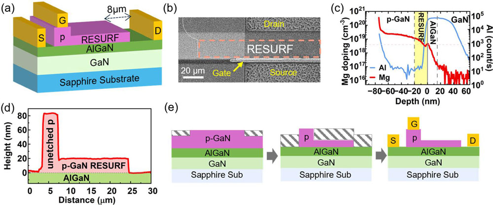
Figure 1: (a) RESURF HEMT 3D schematic diagram. (b) Top-view scanning electron microscope (SEM) image of edge region of fabricated device. (c) Secondary-ion mass spectroscopy (SIMS) profiles for Al and Mg elements in p-GaN/AlGaN/GaN structure. RESURF region (about 20nm above AlGaN surface) marked. (d) Surface morphology profile before contact formation. (e) Main fabrication process steps.
A number of devices with different RESURF dimensions were fabricated. The gate (LG) length was 1.5μm, while the gate–source distance (LGS) was 3.5μm. The drain (D) was separated from the RESURF structure by a distance of 8μm.
The p-GaN was sculpted into the gate/RESURF structure by a two-step dry etch, followed by wet treatments. The first dry etch step was in the source/drain/spacer regions; the second included sulfur hexafluoride (SF6) in the recipe to make the process self-terminating on reaching the AlGaN layer. The wet treatments consisted of tetramethylammonium hydroxide (TMAH) and buffered oxide etch (BOE) rinses designed to reduce surface roughness. The source/drain metals were annealed titanium/aluminium/nickel/gold.
The devices were completed with mesa etching, nickel/gold gate deposition, and passivation with photoresist.
The breakdown voltage for a 17nm-thick RESURF layer (tRES) increased with gate-drain distance, from 810V for 10μm up to 5086V for 35μm. The leakage before the destructive breakdown remained below 0.1μA/mm. The researchers comment that the average breakdown electric field around 1.45MV/cm “is higher than the usual Eave of ∼1MV/cm in the field-plate GaN HEMTs, verifying the effectiveness of the RESURF structure for E-field management.”
The 17nm thickness gave the best performance of the fabricated devices. The team reports: “When tRES ≤ 21nm, BV shows good scalability with the increased LGD, and the highest Eave is observed for tRES = 17nm. When tRES ≥ 26nm, BV can be barely upscaled by LGD, suggesting the presence of a highly non-uniform E-field crowding that leads to premature breakdown and limits breakdown voltage upscaling.”
Extending LGD to 100μm enabled a BV greater than 10kV, the measurement limit of the experimental setup. At this limit, the leakage was still less than 1μA/mm. “These devices can survive repetitive sweeps up to 10kV,” the team adds.
As LGD increases, so naturally does the on-resistance (RON): 17.5Ω-mm for 25μm up to 64.2Ω-mm for 100μm devices. The respective specific on-resistances (RON,SP) were calculated, taking account of the contacts and so on, at 5.9mΩ-cm2 and 69mΩ-cm2, respectively. The sheet resistance in the RESURF region was estimated at 620Ω/□, compared with 450Ω/□ in non-RESURF regions, as calculated from transmission-line model (TLM) measurements. The researchers comment: “This incremental sheet resistance increase is relatively insignificant compared to the substantial breakdown voltage improvement enabled by the RESURF structure.”
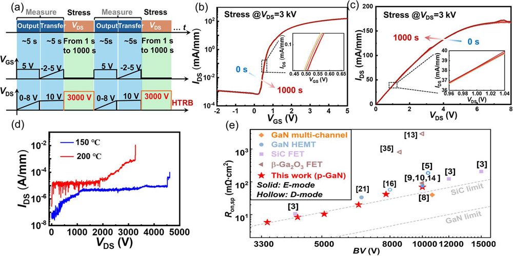
Figure 2: (a) Modified HTRB stress test scheme. Evolution of (b) transfer and (c) output current–voltage (I–V) characteristics during HTRB test. (d) Blocking characteristics of GaN RESURF HEMT at 150°C and 200°C right after HTRB test, 35μm LGD and 17nm tRES. (e) RON,SP-BV trade-off of state-of-the-art SiC, GaN and Ga2O3 transistors with BV above 3.3kV.
The team also performed high-temperature reverse-bias (HTRB) tests to gauge reliability (Figure 2). The researchers claim this as the first report of reliability data for multi-kilovolt GaN transistors. The HTRB used intermittent fast forward I–V sweeps to look for performance degradation. “The device exhibited minimal shifts in both VTH and RON throughout the stress period,” the team reports. After the testing, the breakdown voltage was measured at 150°C and 200°C: 4.5kV and 3.2kV, respectively. “The high-bias leakage current at 150°C is about 20 times higher than the room-temperature counterpart,” the researchers add.
In terms of the on-resistance-breakdown trade-off, the devices showed performance near or beyond the theoretical limit of silicon carbide.
The researchers comment: “Our GaN-on-sapphire RESURF HEMT shows a superior figure-of-merit than SiC and Ga2O3 transistors, at the same time offering a lower wafer cost. In all 10kV GaN devices, our device features an E-mode gate, compatibility with an industry-standard wafer, and the second lowest RON,SP in single-channel HEMTs.”
https://doi.org/10.1063/5.0279059
The author Mike Cooke is a freelance technology journalist who has worked in the semiconductor and advanced technology sectors since 1997.


