


News: Microelectronics
7 August 2025
N-polar deep recess E-mode GaN HEMTs
University of California Los Angeles (UCLA) and University of Michigan Ann Arbor in the USA claim record-breaking small-signal performance for enhancement-mode N-polar deep recess (NPDR) gallium nitride (GaN) high-electron-mobility transistors (HEMTs) [Oguz Odabasi et al, IEEE Electron Device Letters published online 3 July 2025]. In particular, a high 122GHz fT cut-off frequency enabled a high 9.1GHz-μm fTxLG figure of merit despite the short 75nm gate length (LG).
The team sees the device structure as promising for high-frequency, high-power applications. The researchers view the advantages of N-polar GaN as including “intrinsic back-barrier properties, better scalability in gate-to-channel distances, and easier formation of high-quality ohmic contacts”.
The deep recessing enables enhancement-mode/normally-off operation with 0V gate potential representing the off-state. This avoids the risks of “gate bias failures and unintentional activation, particularly in high-voltage applications”. Other advantages of normally-off devices include fail-safety and simpler drive circuit topologies. The team sees potential deployment for power delivery systems in data server and graphics environments.
The NPDR GaN HEMT material was grown by plasma-assisted molecular beam epitaxy (PAMBE), on an N-polar on-axis GaN substrate (Figure 1). The use of an N-polar requires the ALGaN barrier to be below rather than above, as for Ga-polar structures, the GaN channel layer. Unlike for HEMT material grown by metal-organic chemical vapor deposition (MOCVD), the ALGaN was not silicon-doped.
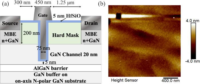
Figure 1: (a) Device schematic, and (b) surface atomic force microscope scan of recessed gate region after ALE and wet etching.
The ohmic source and drain electrodes consisted of MBE n+-GaN regrown without recessing. The device was isolated by a combination of mesa etching and ion implantation.
The deep recess for the gate was achieved by atomic layer etching through a hard mask consisting of plasma-enhanced CVD silicon dioxide, and then wet etching to remove plasma damage. The recess left 5nm of GaN between the gate foot and ALGaN back-barrier.
The hard mask was also used to enable a self-aligned gate deposition process. The gate dielectric was 250°C plasma-enhanced atomic layer deposition hafnium silicate (HfSiO), using a silicon dioxide/hafnium dioxide ratio of 3:2. The gate metal was platinum/gold. The metal for the source/drain contacts was titanium/gold.
The HEMT featured a 75nm gate base length (LG), 450nm ‘T’ top, and 300nm source–gate and 2μm gate-drain distances. The device gate width was 100μm.
In DC operation at +4V gate potential, the peak saturation drain current density was 1.5A/mm, and the knee voltage was 2V. The device threshold was +0.8V, giving an enhancement/normally-off operation mode. The peak transconductance was 550mS/mm at +1.5V gate potential and 3V drain bias.
The team reports: “A gate leakage current of less than 10nA/mm indicates the effective current blocking of the HfSiO gate dielectric. The off-state drain current is ~100μA/mm, due to high buffer leakage. The origin is unknown for now, and will be reduced by further optimizing the epitaxial design.”
The forward-bias gate breakdown was at 6V gate potential and 0V drain. The three-terminal off-state breakdown voltage was around 30V.
Pulsed stressing at 15V followed by measurement at 8V drain bias showed 21% current collapse, seen as “relatively low” by the team. The researchers comment: “Although the dispersion can be further reduced, this work is a significant step toward simplifying the barrier structure compared to the standard MOCVD N-polar GaN HEMTs, which require a combination of composition grading and Si-doping.”
The extrapolated cut-off (fT) and maximum oscillation (fMAX) frequencies from small-signal measurements were 122GHz and 145GHz, respectively (Figure 2). The 75nm device had a fTxLG figure of merit of 9.1GHz-μm. Longer gate lengths enable better channel control and hence higher figures of merit.
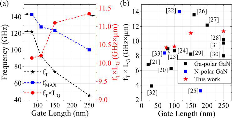
Figure 2: (a) Small-signal results with different gate lengths, and (b) benchmarking of fTxLG of enhancement-mode ALGaN/GaN HEMTs.
Commenting on the benchmark comparison with other works, the team writes: “The device with 75nm LG showed the highest performance compared to devices with similar LG. Devices with other gate lengths in this work also demonstrated top-tier performance. It is worth noting that few enhancement-mode devices in the comparison could support load-pull measurements.”
The researchers performed a Maury passive load-pull study at 10GHz with the quiescent drain voltage (VDQ) and current (IDQ) at 18V and 120mA/mm, respectively, while the quiescent gate potential (VGQ) was +3V (Figure 3).
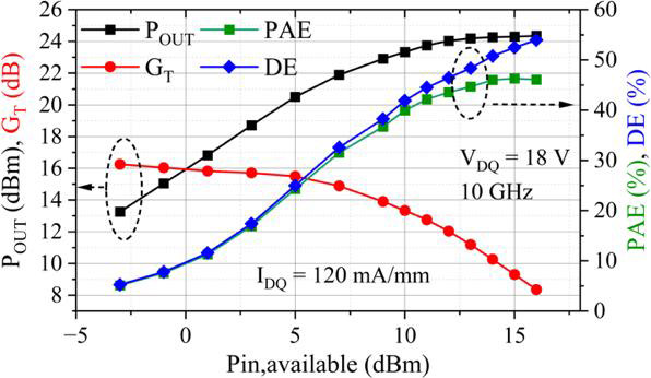
Figure 3: Load-pull results.
The team reports: “With higher VDQ, lower-than-expected VGQ was used, possibly due to drain-induced barrier lowering.”
The output power density was 2.7W/mm, while the drain efficiency (DE) and power-added efficiency (PAE) were 55% and 46%, respectively.
The researchers comment: “A high off-state drain leakage current was observed in these devices and may have contributed to the lower-than-expected efficiency values. Nevertheless, successful load-pull measurements demonstrated impressive results for enhancement-mode operation.”
GaN HEMTs GaN HEMTs PAMBE GaN substrates
https://doi.org/10.1109/LED.2025.3585597
The author Mike Cooke is a freelance technology journalist who has worked in the semiconductor and advanced technology sectors since 1997.


