


News: Microelectronics
21 August 2025
Foundry fabricated AlN-buffer HEMTs
Soctera Inc and Qorvo Inc in the USA have demonstrated high-electron-mobility transistors (HEMTs) fabricated in an RF foundry process with the gallium nitride (GaN) channel sandwiched between ultrawide-bandgap (UWBG) aluminium nitride (AlN) top and back barrier/buffer layers [Reet Chaudhuri et al, Appl. Phys. Express, v18, p076501, 2025]. Such devices have previously been demonstrated in academic laboratory settings, but the researchers report: “These results represent a significant step towards technology maturity for the AlN/GaN/AlN HEMTs by demonstrating their compatibility with current GaN foundry processes.”
They add: “Analogous to how the GaN HEMT technology made the jump from academic research laboratories in the 1990s to the market in the 2000s, this work represents a significant step for the AlN-buffer HEMT technology in taking it closer to being a mature, production-ready candidate for UWBG RF electronics platform of the future.”
The team highlights its work as particularly significant for power amplification systems aimed at Ka-band radio frequencies operating at 27–40GHz, as used in satellite communications networks and high-resolution, close-range targeting radars. The Soctera/Qorvo team also point to potential for 5G cellular networking and data-center deployment.
Another feature of the AlN/GaN/AlN heterostructure profile that could be attractive for these applications is the higher thermal conductivity of AlN: 30% higher compared with GaN. In high-power-density amplification, thermal management becomes a critical factor.
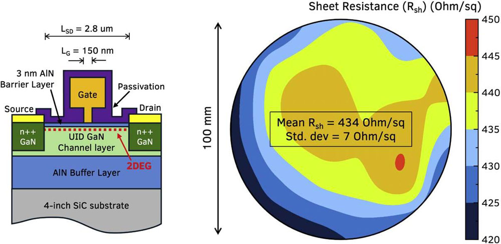
Figure 1: (a) Cross-section scheme for AlN/GaN/AlN HEMT. (b) Uniform sheet resistance map across 100mm wafer measured using transmission line models (TLMs).
A metal-polar heterostructure (Figure 1) was grown using metal-organic chemical vapor deposition (MOCVD) on commercial 100mm silicon carbide (SiC) wafers, typical for GaN-on-SiC RF industrial production. The GaN channel layer was less than 200nm thick. SiC is attractive as a substrate due to its high thermal conductivity, better epitaxial compatibility with the III–nitride material system, and availability in large wafer diameters up to 200mm.
According to TLM measurements, the average sheet resistance Rsh in the two-dimensional electron gas (2DEG) that formed near the AlN barrier layer was 434Ω/□ with a low standard deviation of less than 2%. The result for Lehighton contactless resistance mapping was slightly higher at 442Ω/□ with less than 1.5% variation. Hall measurements reported a 1.26x10¹³/cm2 carrier concentration and mobility of 1248cm2/V-s mobility.
The researchers fabricated a 150nm gate-lenGTh (LG) HEMT with MOCVD-regrown heavily silicon-doped n++-GaN source/drain contact regions with a view to reducing the access resistance to the 2DEG channel to 0.09Ω-mm. The width consisted of two 40μm gate fingers (2x40μm).
The devices achieved an on/off current ratio of order 106 with 643mS/mm peak transconductance (gm). “The maximum value of gm measured on the wafer was 736mS/mm, which is among the highest transconductance values reported in III–nitride semiconductor HEMTs with LG ~150nm, as per authors’ knowledge,” the researchers report. Pinch-off was at −2V, and the maximum drain current was around 1.5A/mm.
The team comments: “The high on-off ratio coupled with the large gm together demonstrate the potential of the 3nm AlN barrier layer for achieving high efficiency, mm-wave operation in RF transistors through vertical and horizontal device scaling.”
Stress testing at 20V drain bias and 0V gate for up to an hour showed a 10% degradation in drain current from around 100mA/mm. The researchers comment: “Preliminary testing showed the devices exhibit minimal degradation, and do not blow-up, indicating the robustness of the AlN/GaN/AlN material.”
The performance under pulsed conditions was similar to reports from academic laboratory studies with current collapse of order 36%, and “substantial drain lag”. The researchers suggest that optimization of the silicon nitride (SiN) passivation could reduce dispersion to around 5% by reduction of surface carrier trapping.
The team adds: “The effect of the surface states on the RF performance could be reduced by moving the surface away from the 2DEG channel, either by growing a thin GaN passivation layer or a crystalline AlN passivation layer.”
These and other methods would need careful study to optimize the various trade-offs.
Small-signal frequency measurements reported cut-off (fT) and maximum oscillation (fmax) frequencies of 45GHz and 174GHz, respectively.
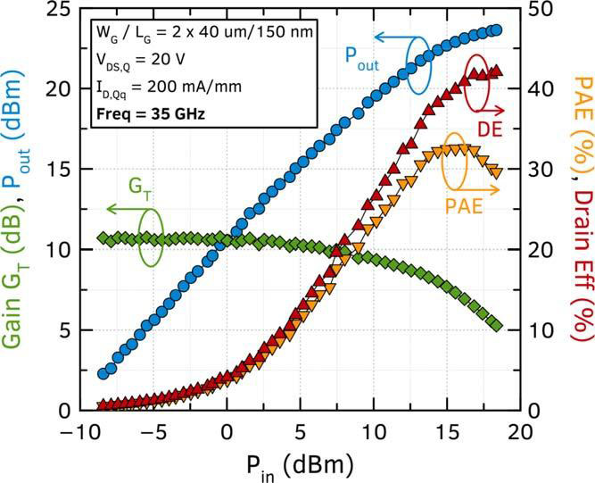
Figure 2: Large-signal load-pull measurement results on AlN/GaN/AlN HEMT.
Large-signal load-pull measurements (Figure 2) used to assess RF power performance showed 32% power-added efficiency (PAE), 2.68W/mm associated power density (Pout), 7.3dB gain (GT) when tuned for peak efficiency. The drain efficiency (DE) reached 42%. Academic demonstrations of the AlN/GaN/AlN HEMTs have previously reported 2.5W/mm power density in the 30GHz range.
The researchers comment: “These are comparable to previously reported Ka-band power output performance from the AlN/GaN/AlN HEMTs. With an uncompressed GT of 11dB, the output power of the HEMT is limited by early onset gain compression from the dispersion from surface states.”
AlN-buffer HEMTs AlN GaN MOCVD
https://doi.org/10.35848/1882-0786/ade6c0
The author Mike Cooke is a freelance technology journalist who has worked in the semiconductor and advanced technology sectors since 1997.


