News: LEDs
7 September 2023
Fabricating 330ppi monolithic GaInN RGB pixels
Meijo University in Japan and King Abdullah University of Science and Technology (KAUST) in Saudi Arabia report on a monolithic stacked red–green–blue (RGB) gallium indium nitride (GaInN) micro-light-emitting diode ( μLED) array with 330 pixel per inch (ppi) density [Tatsunari Saito et al, Appl. Phys. Express, v16, p084001, 2023].
The researchers see the potential for use of such devices in “head-mounted displays and smart glasses for virtual reality, augmented reality and mixed reality”. The micron-level pixels needed for such displays would appear to preclude the use of mechanical assembly techniques, and necessitate the use of monolithic fabrication.
Although GaInN-based LEDs have suffered from severe efficiency problems for longer wavelengths, towards the red end of the visible spectrum there has been recent progress in this area. Further, red GaInN LEDs suffer less from impacts on efficiency from scaling to the smaller device sizes of μLEDs than the usual red LED material, aluminium gallium indium phosphide (AlGaInP).
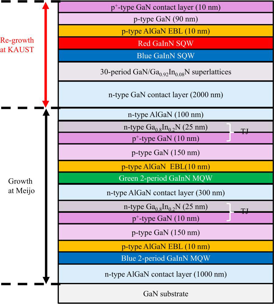
Metal-organic vapor phase epitaxy (MOVPE) was used in two stages to grow the material for the RGB μLED arrays on GaN substrates (Figure 1). First, the blue and green layers were grown at Meijo, while the final red stage was produced at KAUST. The RGB layers were separated by tunnel junctions (TJs).

Figure 1: Schematic cross-section of LED multiple stacked structure.
The red layers were somewhat more involved than the relatively standard blue and green layers. The latter used 2-period multiple quantum wells with suitable-indium-content GaInN alloys.
The red layers included a superlattice, and red and blue single quantum wells (SQWs). The researchers comment: “The blue GaInN superlattice and GaInN SQW inserted between the n-type GaN layer and the active layer in the red LED structure play a role in improving the emission efficiency of the red LED.”
The researchers point out that the GaN substrate used was very expensive, and for production it would be necessary to move to a less expensive material, likely sapphire.

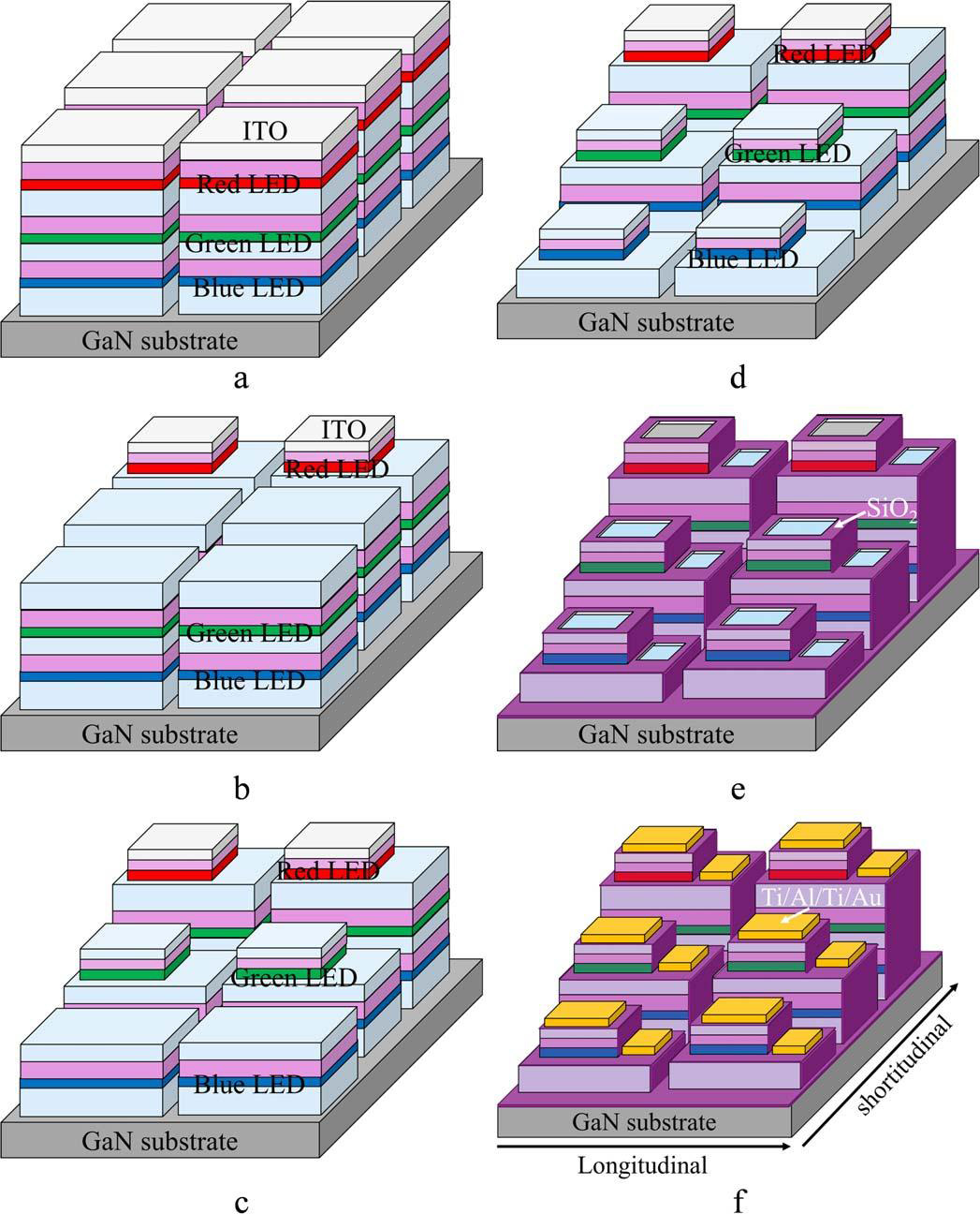
Figure 2: Schematic process flow of μLED array: (a) ITO p-type electrode formation and device separation by etching, (b) red μLED mesa fabrication, (c) green μLED mesa fabrication, (d) blue μLED mesa fabrication, (e) SiO2 passivation film formation, (f) n-electrode formation.
The material was fabricated into RGB pixels with a 330ppi density (Figure 2). The definition of the separate μLED structures was through inductively coupled plasma reactive-ion etch (ICP-RIE). The p-type layers of the TJs were activated through 30-minute annealing at 600°C.
The p-contacts consisted of sputtered indium tin oxide (ITO) transparent conductor, and metal electrodes of titanium/aluminium/titanium/gold (Ti/Al/Ti/Au). The n-electrode was Ti/Al/Ti/Au. Passivation was provided by sputtered silicon dioxide (SiO2).
The μLEDs measured 73 μmx20 μm with 35 μmx15 μm device mesas.
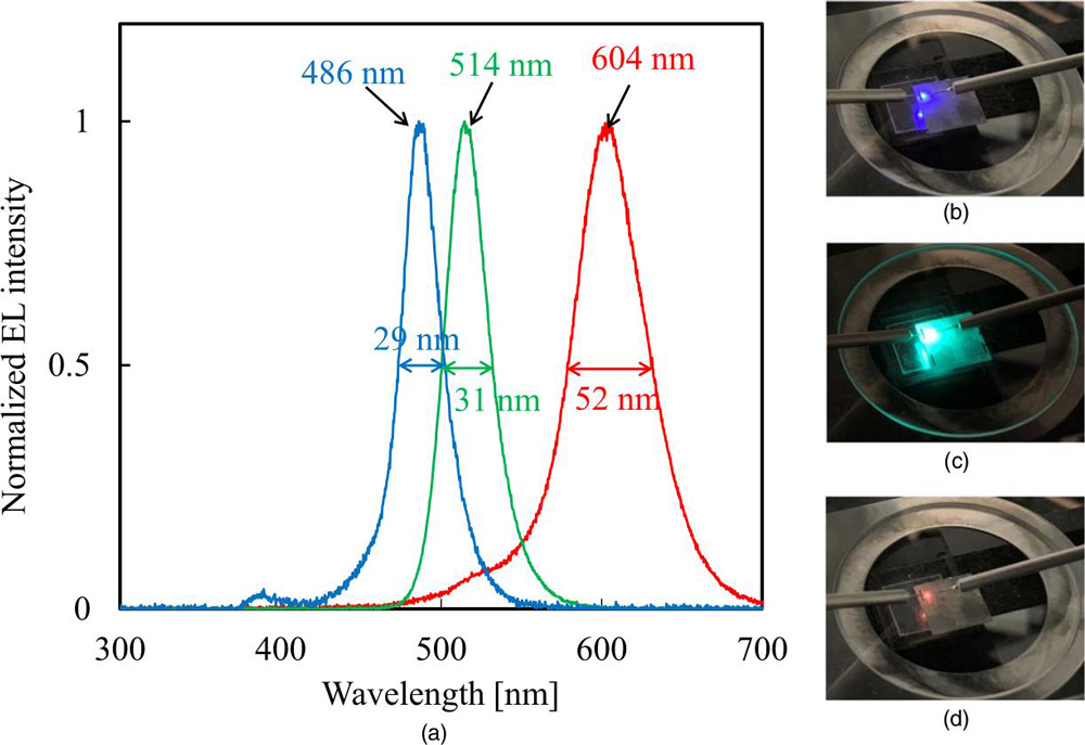
The blue–green–red μLED electroluminescence (EL) spectra, collected from the substrate side with 50A/cm2 injection, peaked at 486nm, 514nm and 604nm, respectively (Figure 3). The corresponding full-widths at half-maximum (FWHMs) were 29nm, 31nm and 52nm. The researchers say that these values are similar to those for separately fabricated devices.

Figure 3: EL spectra of blue–green–red μLEDs; EL photos of (b) blue, (c) green and (d) red μLEDs with a digital camera.
The red and blue device spectra also had sub-peaks around 530nm (green) and 380nm (ultraviolet), respectively. The team comments: “In the future, it should be possible to eliminate the peak at 380nm wavelength from the blue active layer if the growth conditions are optimized by applying the AlN cap layers and lowering the growth temperature of the n-type AlGaN layer to the active layer of blue LEDs.”
The red spectrum also featured a long tail on the short-wavelength side of the peak. “This is not observed when a monochromatic red LED is prepared under the same conditions,” the researchers report, adding: “This could be because the red LED was stacked after the blue and green LEDs, and the optimal crystal growth conditions for the active layer of the red LED were different.”
The turn-on voltages for the blue, green and red μLEDs were 2.8V, 3.2V and 3.2V, respectively, up to 1V greater than the corresponding bandgap energy drops for electrons recombining with hole states to generate photons. The researchers suggest that the smaller electrode areas in the μLEDs may suffer from increased contact resistance on p-type III-N layers.
While the light output power (LOP) from the green μLEDs almost reached 0.8 μW at 10A/cm2 injection, the red and blue LOPs were less than 0.2 μW and 0.1 μW, respectively.
GaInN μLED MOVPE AlGaInP GaInN μLED
https://doi.org/10.35848/1882-0786/aced7c
The author Mike Cooke is a freelance technology journalist who has worked in the semiconductor and advanced technology sectors since 1997.


