News: Optoelectronics
11 October 2023
First droplet epitaxy of InAs quantum dots on InGaAsP quaternary alloy
University of Sheffield in the UK reports the first demonstration of indium arsenide quantum dot (QD) growth on indium gallium arsenide phosphide (InGaAsP, lattice matched to the InP substrate) by droplet epitaxy (DE) [Elisa M. Sala et al, Phys. Status Solidi RRL, p2300340, 2023].
The 1400–2200nm photoluminescence emissions from the resulting QDs cover the low-loss telecom C-band 1530–1565nm, along with other important telecom optical fiber bands, such as O and L. QDs are seen as having strong potential for telecom lasers, pure single-photon and entangled photon pair emissions for quantum information technologies, and for novel nanomemory devices.
The team adds: “The investigation of InAs QD growth embedded in InGaAsP/InP is particularly important given the extensive use of this quaternary alloy as waveguide material for telecom lasers.”
The researchers first studied the formation of indium droplets on a 5nm In0.719Ga0.281As0.608P0.392 layer and their dependence on temperature. The lattice-matched InGaAsP layers were grown by metal-organic vapor phase epitaxy (MOVPE) on InP(100) substrates.
The team found that of the temperatures used droplets only formed for the higher temperatures of 350 °C and 400 °C. Below these temperatures, the trimethyl-indium precursor failed to pyrolyze. At 350 °C and 400 °C, the droplet densities were 3x10⁶/cm2 and 1x10⁶/cm2, respectively. The corresponding diameters/heights were around 425/90nm and 750/105nm.
While droplet formation on InGaAsP at 400 °C had a lower density than either InGaAs (c) or InP (6x10⁷/cm2), the size of the droplets were significantly larger (Figure 1): about 30x wider/10x higher than for InGaAs, and 10x/2x than InP.

Figure 1: Atomic force micrographs of free-standing indium droplets deposited at 400 °C on three different surface types: (a) InGaAs, (b) InP, and (c) InGaAsP. Note different sizes of scan areas adjusted for better visualization.
The team comments: “We ascribe such considerable variation of droplet sizes and densities to a modification of the surface diffusion. From these observations, we can conclude that the InGaAsP surface presents the highest surface diffusion among the three surfaces, which leads to a very low droplet density with the largest size.”
The researchers also point out that (100) InGaAsP features lateral composition modulation (LCM) with GaP- and InAs-rich regions. “Also, greater LCM appears to be correlated with an increased adatom surface diffusion, as this configuration will decrease the adatom incorporation rate,” they add.
To form InAs QDs, the researchers raised the temperature to 520 °C and exposed the droplets to arsine (AsH3). For atomic force microscopy, the QDs were left uncapped. For other work, the QDs were capped with InP.
For InP droplets, no QDs resulted. However, for droplets on InGaAs and InGaAsP there resulted InAs QDs with a higher density than the droplets. The QD densities were 1x10¹⁰/cm2 and 2x10¹⁰/cm2 for the InGaAs and InGaAsP samples, respectively.
Further, the QDs on InGaAsP were much smaller than the initial indium droplets, unlike for the InGaAs-based QDs. “We attribute this to an out-diffusion of indium and redistribution on the InGaAsP surface during the thermal ramp step, which can lead to a reduction in droplet size and a ‘re-wetting’ of the surface,” the team reports.
For lower-temperature droplet deposition samples, the same process resulted in InAs QDs even below 350 °C where there were no indium drops visible on the surface. The researchers explain: “For a droplet temperature of less than 320 °C, the indium precursor trimethyl-indium is not pyrolyzed, i.e. broken down into methyl-indium groups. An increase in temperature during the thermal ramp will trigger a gradual decomposition of methyl-indium occurring at the surface, and providing metallic indium available for droplet formation.”
At 250 °C droplet deposition, the InAs QD density was 8x10⁸/cm2, increasing rapidly to the 1010/cm2 level at higher droplet deposition temperatures. Beyond 400 °C droplet deposition, the researchers found surface degradation to result from increased defect formation.
The team also noted that the process avoided quantum dash formation, i.e. dots elongated in a particular crystal direction, unlike when InAs is deposited on InGaAsP/InP substrates without using droplet epitaxy. The team ascribes this to “the fact that the DE method does not rely on the lattice mismatch between surface and epilayer, thus allowing for a better control of QD formation, which is decoupled from the layer/epilayer mismatch.”
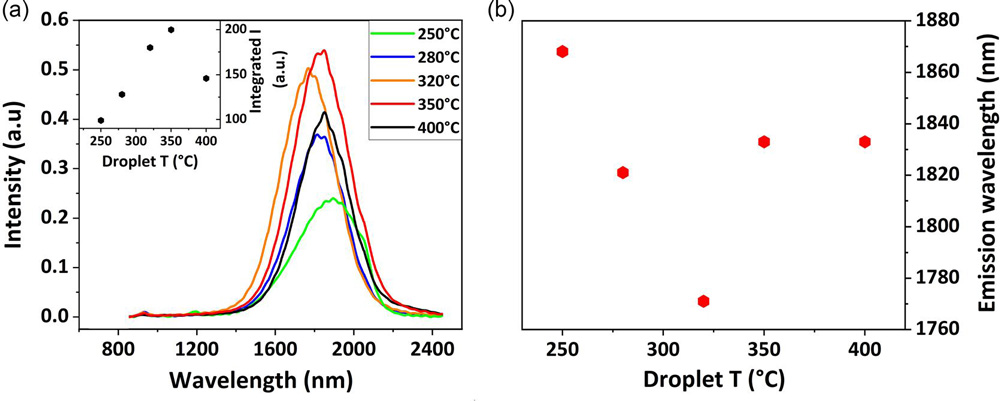
Photoluminescence measurements (Figure 2) showed an increase in intensity up to 350 °C droplet deposition, followed by a sharp decrease at 400 °C. The wavelength range was 1400–2200nm.

Figure 2: (a) Room-temperature photoluminescence of QDs grown with 250–400 °C droplet deposition temperatures (inset: integrated intensity). (b) Peak emission wavelength versus droplet deposition temperature.
Closer study of the dots using 4K low-temperature micro-photoluminescence showed bright single-dot emission in a narrower 1300–1600nm wavelength range.
https://doi.org/10.1002/pssr.202300340
The author Mike Cooke is a freelance technology journalist who has worked in the semiconductor and advanced technology sectors since 1997.


