


News: Photovoltaics
19 October 2023
Fully in-situ roughening for ultrathin III-V solar cells
Colorado School of Mines and the National Renewable Energy Laboratory (NREL) in the USA report on fully in-situ fabrication of light-trapping structures to improve III-V solar cell performance [Allison N. Perna et al, J. Appl. Phys., v134, p135307, 2023].
The structures were generated by texturing the final growth surface through vapor phase etching and re-deposition in the solar cell material growth chamber. The resulting roughened surfaces have high broadband scattering, trapping light for longer in the cell.
The researchers were particularly interested in developing III-V cells with ultrathin absorber layers (less than 400nm). For space applications, this enables higher radiation tolerance and specific power (W/kg), and reduced material content, growth time, and (hence) cost.
The team comments: “Lower manufacturing cost may help expand the market for III-V solar cells to include terrestrial applications where high efficiency and high specific power are paramount.”
Another advantage of thin cells is higher open-circuit voltage due to reduced diffusion recombination. Unfortunately, currents tend to be reduced by increased optical transmission loss. To overcome this, light-trapping schemes need to be implemented. Such schemes are often implemented ex-situ, but as such increase processing times and cost, not least in terms of needing extra capital equipment.
The materials for the Colorado/NREL solar cells were grown using atmospheric-pressure 650 °C dynamic hydride vapor phase epitaxy (D-HVPE) on n-type (100)-oriented gallium arsenide (GaAs:Si) substrates with a 6 ° offcut toward (111) A. The cells consisted of a single junction grown in an inverted sequence, enabling flip-chip fabrication (Figure 1).
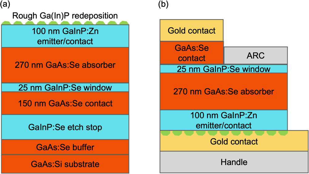
Figure 1: Cell schematics of (a) as-grown inverted cell structure and (b) processed cell structure with nominal layer thicknesses.
The researchers comment: “Inverted cell growth enables in-situ texturing of the rear surface immediately following growth without removal of the sample from the reactor and without requiring subsequent growth on a roughened surface.”
The team also points out that D-HVPE is a high-throughput and potentially lower-cost epitaxial growth technique, and that combining D-HVPE with a fully in-situ texturing method further supports III-V industrial throughput.
The last-grown zinc-doped gallium indium phosphide (Ga0.5In0.5P:Zn) layer was grown with a thickness that maintained a 100nm emitter/contact layer after texturing with in-situ etching/re-depostion in the reaction chamber.
The researchers used a dual-growth reactor, where the process conditions for the next layer are prepared in one chamber, while the growth proceeds in the other. The last etch/texturing step involved hydrogen chloride (HCl), phosphine (PH3), or both gases in hydrogen carrier gas. These gases were also used in the growth of GaInP.
In separate experiments to tune the etch/re-deposition texturing, it was found that HCl on its own resulted in a mirror-like surface, similar to the initial GaInP layer, without generating the desired texturing.
The team reports on the effect of adding PH3: “In contrast to the planar etching observed while using only HCl, the addition of PH3 to the HCl vapor etch led to a rough textured surface with low broadband specular reflectance that is potentially useful as a broadband scatterer.”
Changes in texturing quality were studied by varying the process duration and HCl flow rate. Studies using scanning electron microscopy, Auger electron spectroscopy (AES), cross-sectional scanning transmission electron microscopy with energy-dispersive spectroscopy (STEM-EDS), and high-resolution x-ray diffraction (HRXRD), found the texturing to result from etch and re-growth of Ga(In)P (highly Ga-rich GaInP).
The researchers comment: “The observation that the textured morphology does not form from HCl etching alone and does form with supplied PH3 suggests that re-deposition and island growth of Ga(In)P result from reactions between etch products and the supplied PH3.”
The material used for solar cells was textured using a HCl/PH3 flow rate of 4/8 standard cubic centimeters per minute (SCCM) at 0.0008/0.0110atm partial pressures, respectively. The texturing time was 60 seconds.
Cell fabrication began with electroplating gold onto the textured surface. The device was then flipped onto a silicon handle substrate. The active area of the cell was about 0.25cm2. The flipped cell also included a magnesium fluoride/zinc sulfide (MgF2/ZnS/MgF2) anti-reflective coating (ARC) on the window area. The performance was compared with a cell without texturing (Figure 2).
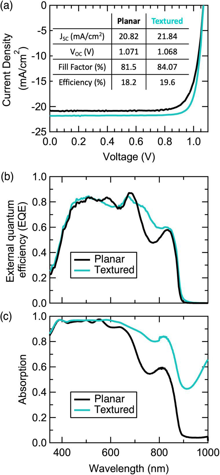
Figure 2: Cell measurements of thin solar cells without texturing (black) and textured (blue): (a) current density versus voltage; (b) external quantum efficiency; (c) absorption.
The best of four devices for each type showed a 4.9% increase in short-circuit current density (JSC) for the textured structure. Averaged over the four samples the increase was 5.1%.
The external quantum efficiency (EQE) performances were similar for the two device types, apart from some oscillations for the planar type arising out of Fabry–Pérot interference effects. The textured cell efficiency was 19.6%, compared with 18.2% for the control planar device.
The researchers comment that there is no appreciable loss in open-circuit voltage VOC or fill factor, “indicating similar material quality and no adverse effect on the back contact metallization, respectively.”
The absorption (A) of the cells was calculated from total hemispherical reflectance (Rh) data from UV-Vis measurements in an integrating sphere (A = 1–Rh).
The researchers report: “We observe a lower EQE than absorption in both cells that, for the textured cell, is more significant at long wavelengths. This may be due to parasitic absorption in the rough gold surface, causing the metal to act as a lossy mirror.”
In an ideal cell, the two quantities would be equal, suggesting losses either due to optical absorption or recombination of carriers into photons. The team suggests that improving the rear-side metallization process could result in lower losses and increased current.
https://doi.org/10.1063/5.0160559
The author Mike Cooke is a freelance technology journalist who has worked in the semiconductor and advanced technology sectors since 1997.


