


News: Microelectronics
26 October 2023
RF sputtering of gallium oxide on diamond
Researchers based mainly in Japan report “the first achievement in hetero-epitaxial growth of β-Ga2O3 thin films on single-crystalline diamond (111) wafers using RF magnetron sputtering” [Takafumi Kusaba et al, Applied Physics Express, v16, p105503, 2023]. While β-Ga2O3 is a promising new material for extreme-condition electronics, it suffers from a low thermal conductivity. Growing Ga2O3 on high-thermal-conductivity single-crystal diamond (SCD) could enable devices with self-thermal management.
The team consisted of researchers from Kyushu University, National Institute of Advanced Industrial Science and Technology (AIST), Kyushu Institute of Technology in Japan, and one from Aswan University in Egypt and the Center for Japan–Egypt Cooperation in Science and Technology (E-JUST Center) in Japan.
The researchers see their work as supporting “further research on scalable β-Ga2O3/diamond hetero-structures for future electronic and optoelectronic applications with not only high performance but also good self-thermal management”.
Among the material properties of β-Ga2O3 giving rise to these hopes are a wide bandgap of 4.5–4.9eV, high breakdown field (~8MV/cm), resistance to chemical damage, and an ability to withstand high levels of radiation and thermal stress. The thermal conductivity is in the range 10–30W/m-K, while that of diamond is around 2000W/m-K.
An added attractive possibility for the combination of β-Ga2O3/diamond hetero-structures is the easy p-type doping of diamond with boron, since at present there is no feasible method for arranging p-type Ga2O3, which is naturally n-type.
Techniques such as van der Waals and wafer bonding of β-Ga2O3 on diamond have previously been reported, but not direct-growth processes like RF sputtering. Direct growth methods tend to be preferred for scalable manufacturing and lower costs.
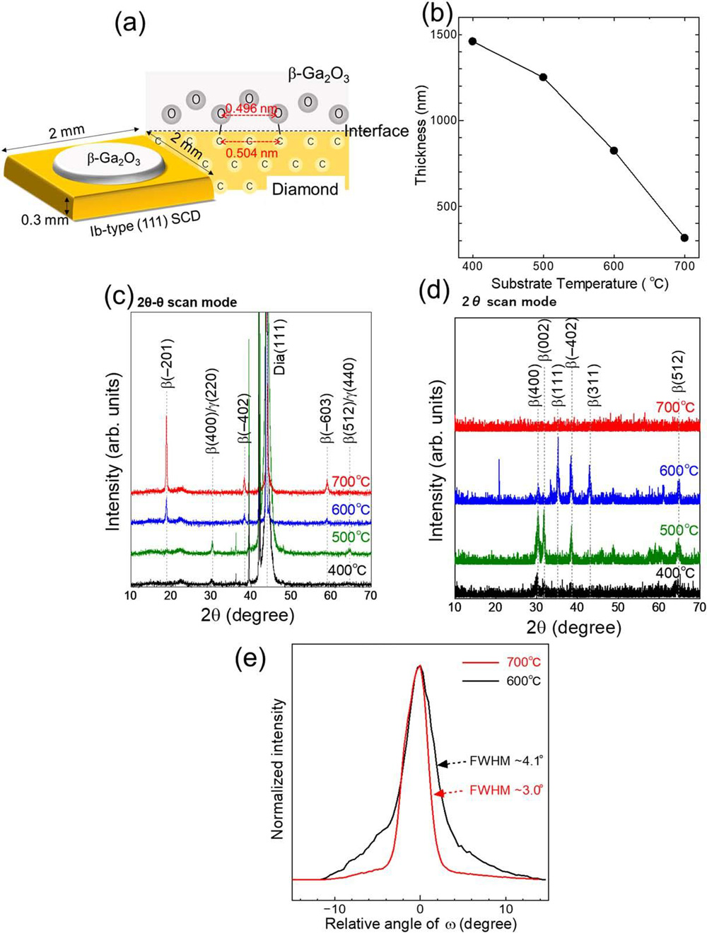
Figure 1: (a) Structural drawing of RF sputtered β-Ga2O3 thin film grown on SCD (111) and expected atomic bonding between oxygen and carbon atoms at Ga2O3/diamond interface. (b) Relationship between grown film thickness and substrate temperature. (c,d) X-ray diffraction (XRD) patterns from 2θ−θ and 2θ scan modes, respectively. (e) XRD rocking curves of (−201) peak for the samples grown at 600°C and 700°C.
The radio-frequency magnetron sputtering (RFMS) was carried out using a commercial undoped Ga2O3 target and Ib-type (111) SCD substrate from Sumitomo Corp in Japan (Figure 1). The RFMS growth pressure was 1.5x10⁻¹Pa. The atmosphere in the chamber was supplied by an argon flow without oxygen. The RF power was 50W, and the deposition time was 48 hours. The β-Ga2O3 was grown in a circular region defined by a metal mask.
While the growth rate slowed significantly at the higher substrate temperatures (315nm for the 700°C material), the Ga2O3 crystal quality at lower temperatures deteriorated. Indeed, at 400°C the material appeared to be amorphous, according to x-ray diffraction (XRD) analysis. The 500°C sample consisted of mixed β- and γ-phase Ga2O3. The 600°C and 700°C film were unmixed β-Ga2O3. However, the 600°C material was polycrystalline with a number of different plane orientations. The 700°C sample was mainly (−201) oriented with a significantly narrower rocking curve peak, according to the full-width at half maximum (FWHM) of 3.0°, compared with 4.1° for the 600°C material.
The researchers comment: “The higher substrate temperature promotes the β-phase crystallization of Ga2O3 and reduces the diamond surface energy, which stimulates the mobility of adatoms to migrate on the diamond terraces, improving the capability of the layer-by-layer growth process.”
The lattice mismatch between the diamond (111) and β-Ga2O3 (−201) was in the range −1.6–2.2%, according to pole-figure XRD analysis, comparable to β-Ga2O3/sapphire (1.7–4.8%).
The team comments further on their pole-figure analyses: “Two unique planes, including (−202) and (002), of (−201) β-Ga2O3 texture parallel to the (111) diamond texture with six different in-plane rotation domains were found.”
SEM inspection (Figure 2) of the sample surfaces showed mountain-liked crystals on the surface of the film grown at 700°C. The team explains: “These surface structures may indicate that β-Ga2O3 thin films were grown on SCD (111) substrates by the Stranski–Krastanov (S–K) growth mode, in which the two-dimensional (2D) mode occurs in the early stages of growth and then it changes to three-dimensional (3D) island growth when the critical thickness of the grown film is exceeded. Optimization of the film thickness is required to further flatten the surface of β-Ga2O3 thin films grown on SCD (111).”
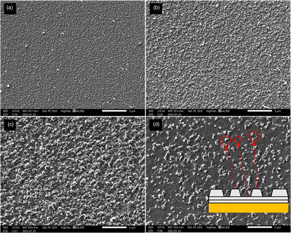
Figure 2: Top-view scanning electron microscope (SEM) images of thin films grown at different substrate temperatures: (a) 400°C, (b) 500°C, (c) 600°C and (d) 700°C. Inset: (d) drawing of film structure grown under S–K mode.
The researchers also used x-ray photoelectron spectroscopy (XPS) to determine the elemental ratios in the film at the different growth temperatures. The sample grown at 700°C had a O/Ga ratio of 1.31, closest of all the samples to the 1.5 of perfect Ga2O3. The other temperatures result in O/Ga of less than 1.16.
The team comments: “Overall, these XPS results suggested that a high-substrate-temperature deposition by sputtering is effective in suppressing the generation of oxygen defects and an acceptable atomic composition of β-Ga2O3 thin films grown on SCD (111) substrates could be achieved by using a substrate temperature of 700°C.”
The author Mike Cooke is a freelance technology journalist who has worked in the semiconductor and advanced technology sectors since 1997.


