


News: LEDs
23 November 2023
Stacking p-down green LEDs using tunnel junctions
Ohio State University and Lumileds LLC in the USA, report on dual-junction p-down green light-emitting diodes (LEDs) [Sheikh Ifatur Rahman et al, Jpn. J. Appl. Phys., vol62, p110904, 2023].
By connecting stacked active LED regions with tunnel junctions, the researchers reduced the injection current needed for a desired light output power. A reduced injection current allows the devices to operate in a region with higher external quantum efficiency (EQE), avoiding the efficiency droop typically seen at higher currents.
Efficiency droop becomes particularly severe in longer-wavelength green LEDs, creating a ‘green gap’ for efficient semiconductor light-emission capabilities for lighting, display and laser applications. With further development, it should be possible to stack more than two LED active regions.
Further, the use of the p-down structure should avoid the efficiency sapping effects of the charge polarization field that arises from the contrasting ionicity of the chemical bonds in the different layer materials that make up the devices.
The researchers explain: “In conventional metal-polar (+c oriented) LEDs, where the p-doped layer is on top of the n-doped region, the polarization dipole within the InGaN quantum well opposes the depletion field, and high electrostatic carrier injection barriers are formed on both sides of the well. These barriers block electron and hole injection into the active region, and therefore could cause degradation in the electrical efficiency of the diode. In the p-down case, the polarization dipoles are in the same direction as the depletion field and, therefore, the electrostatic barriers to electron and hole injection at the edge of the quantum wells are reduced.”
In the p-down format the charge polarization field is reversed relative to the device structure. Of course, the conventional structure is conventional due to a number of difficulties in realizing the p-down structure, particularly in activating the buried p-type layers.
Activation usually consists of thermally annealing the magnesium-doped gallium nitride (GaN) to drive out hydrogen, which passivates the p-doping effect of Mg. When p-GaN is the top layer, most of the hydrogen escapes from the top surface. In buried p-GaN, the only route is through the sidewalls, making activation more tricky.
More problems arise from the thermal budget. High-temperature processing can affect doping profiles and degrade the light-emitting indium gallium nitride (InGaN) quantum wells (QWs).
The epitaxial material for the p-down LED with two active regions was grown using metal-organic chemical vapor deposition (MOCVD) on n-GaN/sapphire templates (Figure 1). The active light-emitting regions contained two InGaN QWs separated by GaN quantum barriers (QBs). The tunnel junctions consisted of heavily-doped p/n layers. The bottom junction enables uniform current spreading across the device in the more electrically conductive n++-type layer.
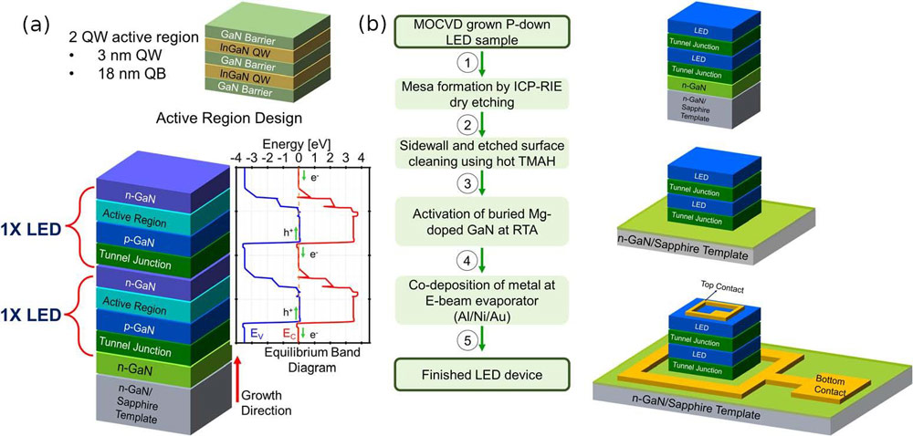
Figure 1: (a) Epitaxial structure of dual-active-region p-down LED with active region design and corresponding equilibrium band diagram. (b) Process flow for single-junction and dual-junction p-down LEDs.
The material was fabricated into LEDs, using direct-write optical lithography, inductively coupled plasma reactive-ion etch (ICP-RIE), rapid thermal annealing (RTA), and electron-beam (E-beam) evaporation. The ICP-RIE was used for mesa isolation, while the RTA activated the buried p-GaN layers. The E-beam evaporated contact metals were aluminium/nickel/gold (Al/Ni/Au) on n-GaN. The devices were not optimized for light extraction — for example, the metal contact was not designed with a view to high reflectivity. The devices measured 100μmx100μm.
The forward voltages at 20A/cm2 were 3.6V and 7.1V for single- and dual-LED devices, respectively. The 3.6V/junction excess voltage is relative to the ~2.3eV photon energy. The researchers comment: “We attribute the excess voltage in each single p-down LED+TJ structure to the tunnel junction — MOCVD-grown tunnel junctions in the n++/p++configuration have high voltage drop due to challenges associated with achieving high Mg doping density in the top p-region while ensuring that the active region does not degrade due to the Mg doping tail. The estimated tunnel voltage drop in these devices is still the lowest voltage demonstrated for any MOCVD-grown reversed-polarization tunnel junction-based green LED.”
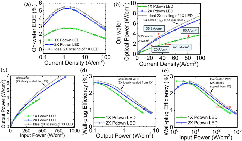
Figure 2: (a) On-wafer measured EQE for single-junction and dual-junction devices. (b) Optical power. (c) Electrical input power and output optical power. (d), (e) Calculated wall-plug efficiency with corresponding output power and input power.
The peak emission wavelengths varied in the range 543-517nm for current densities in the range 0.1–100A/cm2, respectively. The EQEs at 1A/cm2 injection reached 2.75% and 5.3% for the single- and dual-junction LED, respectively (Figure 2). At 100A/cm2 the corresponding EQEs were reduced to 1.4 and 2.5%.
The team comments: “While the scaling of EQE is not exactly 2x, the significant improvement of the EQE value both at low and high current densities highlights the benefits of cascading multiple active regions to tackle pronounced efficiency droop in long-wavelength emitters. Several factors such as the increased thermal budget and Mg memory effects can impact the optical characteristics of multi-active-region LEDs and cause non-ideal EQE scaling.”
For 2W/cm2 optical output power density, the single-junction LED required a 42.5A/cm2 injection, while the dual-junction device only needed 20A/cm2. The researchers calculate the single- and dual-LED wall-plug efficiencies (WPEs) at 2W/cm2 output to be 1.17% and 1.40%, respectively.
At 3.25W/cm2 output, the corresponding current densities were 80A/cm2 and 36.2A/cm2. The lower injection currents for the dual-junction device enabled it to operated in a more efficient region for producing light.
https://doi.org/10.35848/1347-4065/ad07fa
The author Mike Cooke is a freelance technology journalist who has worked in the semiconductor and advanced technology sectors since 1997.


