


News: LEDs
1 November 2023
Extracting efficiency contributions for sub-10μm LEDs
Universtité Grenoble Alpes, CEA-LETI in France has used cathodoluminescence (CL) to disentangle the size-dependence of the various sub-10μm indium gallium nitride (InGaN) light-emitting diode (LED) efficiencies [Palmerina González-Izquierdo et al, ACS Photonics, published online, 16 October 2023 ].
The team reports: “Our results show that, for small μLEDs (between 2.5μm and 10μm width), there is an optimal intermediate LED size for which the light emission is maximized, which we attribute to a competition between the light extraction efficiency (LEE) (which decreases with LED size) and the internal quantum efficiency (IQE) (which increases with LED size). In contrast to most prior studies that typically examine either the IQE or LEE with respect to size for larger LEDs, our work stands out by examining the interplay between IQE and LEE for μLEDs below 10μm.”
Researchers have recently been developing μLEDs particularly for display applications in competition with liquid-crystal and organic LED products for micro-displays for augmented reality and virtual reality. Other potential applications include visible light communication, and optogenetics where cell activity can be controlled by light.
By separating the LEE and IQE contributions to the external quantum efficiency (EQE) and finding their respective dependence with size and geometry, the Grenoble Alpes, CEA-LETI team hopes to pave the way toward the efficient miniaturization of μLEDs.
The team grew InGaN-based LED heterostructures on 200mm-diameter silicon (Si) (111)-oriented substrates by metal-organic vapor phase epitaxy (MOVPE). The active light-emitting region consisted of multiple quantum wells (MQWs) with 5 layer pairs of 2nm/8nm InGaN/GaN wells/barriers.
The structure included n- and p-type GaN layers, an aluminium gallium nitride (AlGaN) electron-blocking layer, and a top layer of transparent indium tin oxide (ITO) conductor, as usual for epitaxial material aimed at LED production.
The researchers etched the material into square and circular μLED mesa structures by inductively coupled plasma (ICP). To enable cathodoluminescence (CL) analysis, the ITO layer was removed in a wet process involving hydrofluoric and hydrochloric acids.
The CL excitation used a focused 10keV electron beam with a 12nm current. A light microscope embedded within the electron objective lens collected data over a 200μm area. Monte Carlo simulations were used to find the best electron-beam energy to probe the MQW structure.
An advantage of using a silicon substrate for the CL study was that it absorbed the emitted light, virtually eliminating cross-talk between the excitation responses from the different regions of the mesas, unlike for transparent substrates like sapphire where reflections occur at the interfaces between materials with different refractive indexes.
The researchers first looked at the CL response at room temperature (RT) across the various square or circular mesas (Figure 1). The data were normalized to the highest value for each shape, and averaged over a strip about a path through the mesa center. The path for the square mesas was parallel to one side. The diameters/sides of the mesas were 2.5μm, 5.0μm, 7.5μm and 10.0μm.
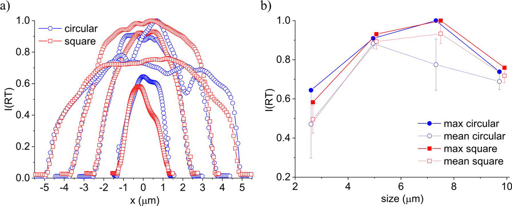
Figure 1: (a) Integrated MQW CL profile at RT for four different sized square/circular mesas. (b) Maximum (filled markers) and mean (empty markers) intensity over the central area of the mesas obtained from graph a.
One observation made was that the maximum CL intensity was reached within about 3.5μm of the edges of the largest mesas. The team points out that this is greater than the minority carrier diffusion length in GaN (0.1–1μm) or InGaN. Since the smaller mesas were less than 7μm, “the whole volume is affected by non-radiative recombination through sidewall defects,” the researchers comment.
The team points out that there seemed to be a problem with their 7.5μm circular mesa structure, as indicated by the large standard deviation in mean CL intensity of the central mesa region.
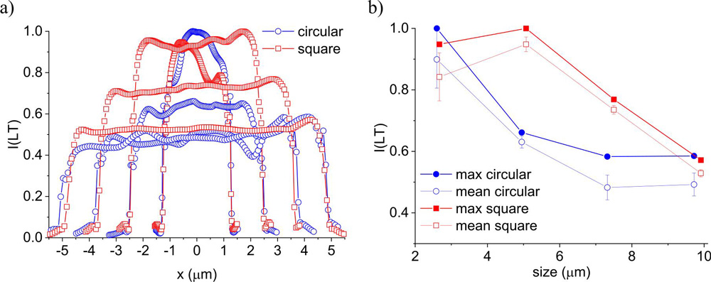
Figure 2: (a) Integrated MQW CL profiles at 10K. (b) Maximum (filled markers) and mean (empty markers) intensity over central area from graph a.
The researchers then compared the RT results with those obtained at the low temperature (LT) of 10K (Figure 2). While the RT CL data are considered to be an indication of the trend of EQE, those at low temperature are seen as representing LEE, given that the LT IQE is expected to be near 100%. The idea of using LT data to represent LEE results from the theoretical expectation that non-radiative routes to electron recombination with holes are frozen out. In particular, the temperature dependence of the Shockley–Read–Hall (SRH) model for non-radiative recombination of conduction-band electrons through defect levels to holes in the valence band suggests this.
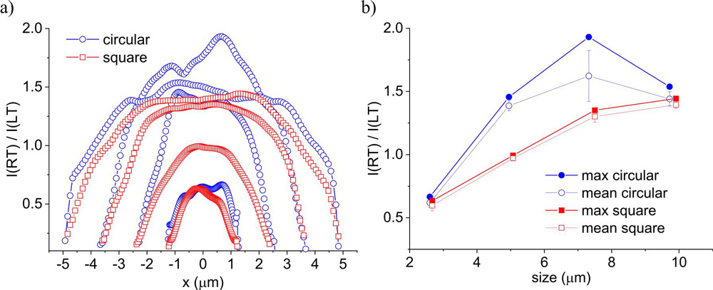
Figure 3: (a) MQW I(RT)/I(LT) profile from normalized intensities. (b) Maximum (filled markers) and mean (empty markers) value over the central area of the mesas obtained from graph a.
The IQE is given by EQE/LEE; and LEE is expected to be roughly independent of temperature. The ratio of the CL intensities, I(RT)/I(LT), is thus expected to be proportional to the IQE at room temperature (Figure 3).
The CL results suggest opposing trends for LEE (Figure 2) and IQE (Figure 3) with size — decreasing and increasing, respectively. For circular mesas, Figure 3 might suggest an optimum IQE near 7.5μm diameter and a sharp decline for 10μm, but the Grenoble Alpes, CEA-LETI team urges caution: “The CL intensity values measured for the 7.5μm size at room temperature exhibit a broad distribution, as seen in the mean and standard deviation presented in [Figure 2]. Consequently, caution must be exercised in drawing conclusions regarding whether this decrease represents a genuine decline or a dampening effect similar to that observed in the case of square mesas.”
The researchers conclude: “These analyses show that the optimal light emission for the intermediate-sized 7.5μm mesa structures at room temperature can be explained by an interplay between the LEE and the IQE for both geometries: the LEE decreases with the size of the mesa, while the IQE is governed by non-radiative recombination through sidewall defects, which affects the mesas with a higher perimeter-to-surface ratio the most.”
https://doi.org/10.1021/acsphotonics.3c00971
The author Mike Cooke is a freelance technology journalist who has worked in the semiconductor and advanced technology sectors since 1997.


