


News: LEDs
16 November 2023
Full-color active-matrix micro-LED micro-displays
Hong Kong University of Science and Technology in China reports progress in fabricating prototype full-color active-matrix micro-LED micro-displays with 391 pixels per inch (ppi) density and “decent” color gamut [Longheng Qi et al, Light: Science & Applications, v12, p258 2023].
The 200x80-resolution device consisted of indium gallium nitride (InGaN, blue/green) and aluminium gallium indium phosphide (AlGaInP, red) micro-LED arrays flip-chip bonded to a silicon (Si) complementary metal oxide semiconductor (CMOS) backplane.
Such micro-display formats are being developed for augmented-reality/mixed-reality (AR/MR) application.
The researchers comment: “The performance of the current prototype is limited by the yet-to-be-optimized GaN-on-Si dual-wavelength LED epiwafers and the CMOS driver”. A further concern is yields, “primarily determined by the integration step of the monolithic AlGaInP red micro-LED array.”
The 200x80 (0.55-inch diagonal) full-color (RGB) displays were constructed from flip-chip bonding of InGaN blue/green and AlGaInP red micro-LED arrays (Figure 1). The dual-color InGaN devices generated their light from multiple quantum wells (MQWs) consisting of three bottom blue wells, a single green well, and two top blue wells. The InGaN LED structure was grown on a 4-inch silicon substrate.
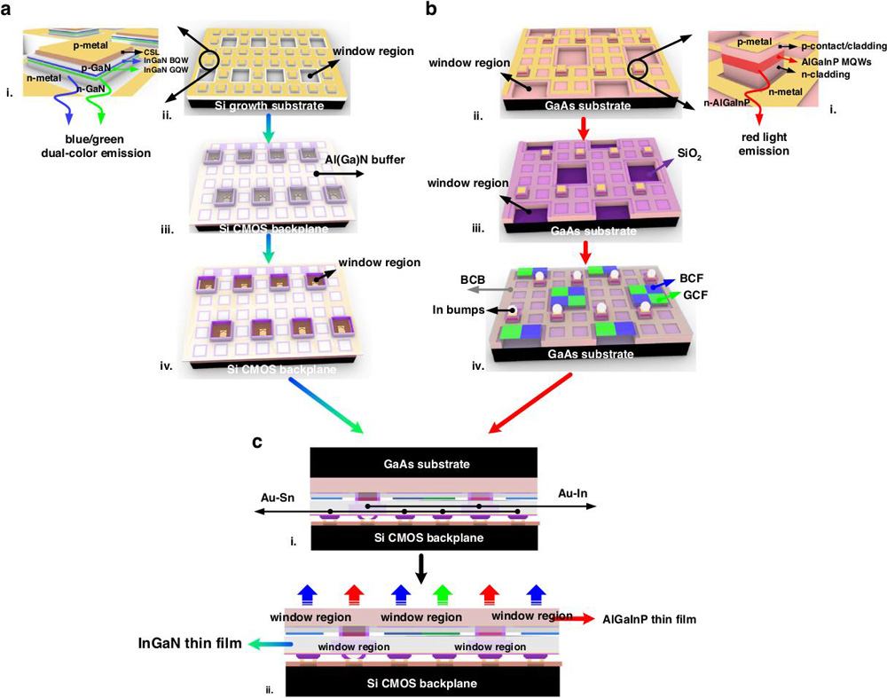
Figure 1: Process flow. (a) Fabrication of InGaN blue/green dual-color micro-LED display: (i) subpixel; (ii) window regions and p, n metallization; (iii) Au–Sn flip-chip bonding to CMOS backplane; (iv) Al(Ga)N buffer etchback. (b) Fabrication of AlGaInP red micro-LED array: (i) subpixel; (ii) window regions and p, n metallization; (iii) SiO2 passivation and contact holes; (iv) BCB polymer etchback, reflow of indium micro-bumps and blue/green color filter patterned. (c) Heterogeneous integration: (i) Au–In flip-chip bonding of InGaN and AlGaInP display arrays; (ii) GaAs substrate removal.
The InGaN blue/green array of 15μmx15μm subpixels was flip-chip bonded to a backplane with electronics consisting of three-transistor-one-capacitor (3T1C) pixel drivers. The solder bumps were tin/gold (Sn/Au). The silicon growth substrate was removed.
The AlGaInP red array was grown on gallium arsenide (GaAs) substrate. Window regions measuring 50μmx50μm were etched in the structure so that, when the chip was flipped onto the InGaN/backplane assembly, blue/green light could transmit out of the device. Patterened blue (BCF) and green (GCF) color filters were applied in the windows to create blue and green subpixels.
After bonding with indium solder bumps, the GaAs growth substrate was removed. An epoxy underfill process was used to support the fragile AlGaInP thin film, avoiding cracking and improving its mechanical strength. Curing the epoxy further enabled a crack-free robust AlGaInP thin film.
The researchers comment: “The Au–In bonding of the red micro-LED array has a lower soldering temperature (180°C) than the Au–Sn bonding (220°C) so that it will not damage the as-fabricated InGaN dual-color display structures.”
The color balance of the blue/green InGaN pixels was controllable by the injection current density: pure green below 0.12A/cm2 with the blue peak becoming dominant beyond 0.37A/cm2. In terms of voltage, the switch point was at 2.60V. The full-widths at half maximum (FWHMs) were 20nm and 33nm for the blue and green peaks, respectively. The corresponding peak wavelengths were around 444 and 520nm.
The narrower bandgap of the green wells explains how the emissions begin from them. “With the increase of carrier injection, more carriers fill and recombine both in the top blue and green QWs so that the blue peak gradually occurs and increases together with the green peak,” the team adds.
Tests on the red AlGaInP showed a drive current of 3μA at 1.70V. The peak wavelength was at 628nm with current injection in the range 0.14–1.74A/cm2. The FWHM was around 18nm.
When integrated into the full-color format, the InGaN section maintained its performance, but the AlGaInP array did suffer from resistance degradation after the GaAs substrate removal (Figure 2). The researchers suggest that possibly “the current conduction path in the array is limited in the several-microns-thick n-AlGaInP layer after removal of the thick conductive GaAs substrate.”
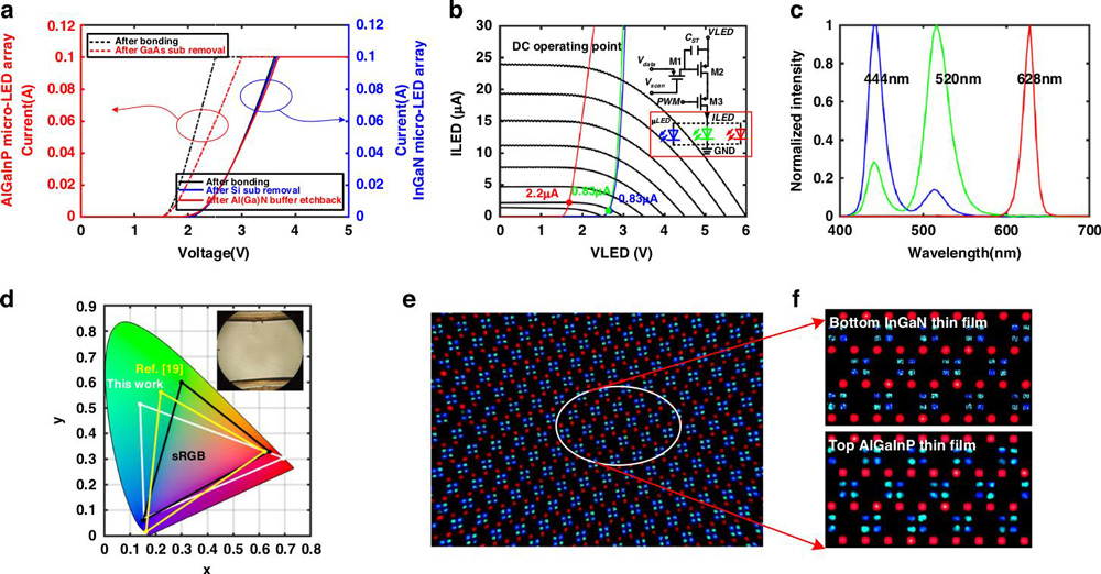
Figure 2: (a) Current–voltage (I–V) curves of InGaN dual-color micro-LED array and AlGaInP red micro-LED array during integration. (b) Pixel driver output curves and I–V curves of micro-LED subpixels. (c) Elecroluminescence spectrum of full-color display at 3.2V, aiming at current injections of 0.83 and 2.2μA for the blue/green and red subpixels, respectively. (d) Color gamut in CIE 1931 chromaticity diagram (Inset: as-fabricated double-layer thin-film full-color display). (e) Inspection of all RGB subpixels turned on. (f) Zoomed-in photos at different focal planes.
The researchers report: “Compared with our previously reported work using the QDs-photoresist color conversion method [the Ref. 19 referred to in Figure 2], this heterogeneously integrated full-color display presents better red emission, with less ideal blue and green color performance.”
The brightness of the individual subpixels was controlled using pulse-width modulation (PWM), allowing different colors to be rendered.
LED micro-displays LEDs AlGaInP InGaN GaAs substrate
https://doi.org/10.1038/s41377-023-01298-w
The author Mike Cooke is a freelance technology journalist who has worked in the semiconductor and advanced technology sectors since 1997.


