


News: Microelectronics
30 November 2023
Record frequency AlGaN-channel transistors
Cornell University in the USA claims a record high speed for any aluminium gallium nitride (AlGaN)-channel transistor from an AlN/AlGaN/AlN quantum well (QW) high-electron-mobility transistor (HEMT) structure [Eungkyun Kim et al, Appl. Phys. Express, v16, p11100, 2023].
The Cornell team reports unit-gain cut-off (fT) and maximum oscillation (fmax) frequency values of 67GHz and 166GHz, respectively. The team comments: “This translates to the geometric mean of fT and fmax exceeding 105GHz, breaking the 100GHz barrier for the first time for AlGaN-channel HEMTs.”
The researchers attribute the high speed to a low contact resistance and aggressively scaled gate length and source-to-drain distance, overcoming somewhat the impact of the higher sheet resistance of AlGaN from alloy scattering. The shorter gate length ensures that the carriers under the gate are velocity-saturated, and reducing the source-to-drain distance decreases access resistance.
The wider bandgap of AlGaN over existing GaN-channel HEMTs should result in higher breakdown voltages, and indeed rapid progress is being made for long AlGaN-channel transistors aimed at relatively low-frequency power-switching application. Combined with higher frequency performance, AlGaN HEMTs have the potential to deliver higher-power-density systems.
The material for the AlN/Al0.25Ga0.75N/AlN QW HEMTs was grown by plasma-assisted molecular beam epitaxy on semi-insulating silicon carbide (6H-SiC) substrate. The AlGaN well was 24nm, surrounded by AlN barriers consisting of 1μm buffer and 15nm top layers. Hall measurements gave electron charge density and mobility values of 3.05x10¹³/cm2 and 45cm2/V-s in the two-dimensional electron gas (2DEG) channel.
The material was fabricated into HEMTs with T-gate and silicon nitride (SiN) passivation (Figure 1). Electron-beam lithography was used to define the gate region. The passivation was designed to improve dispersion control of the device.
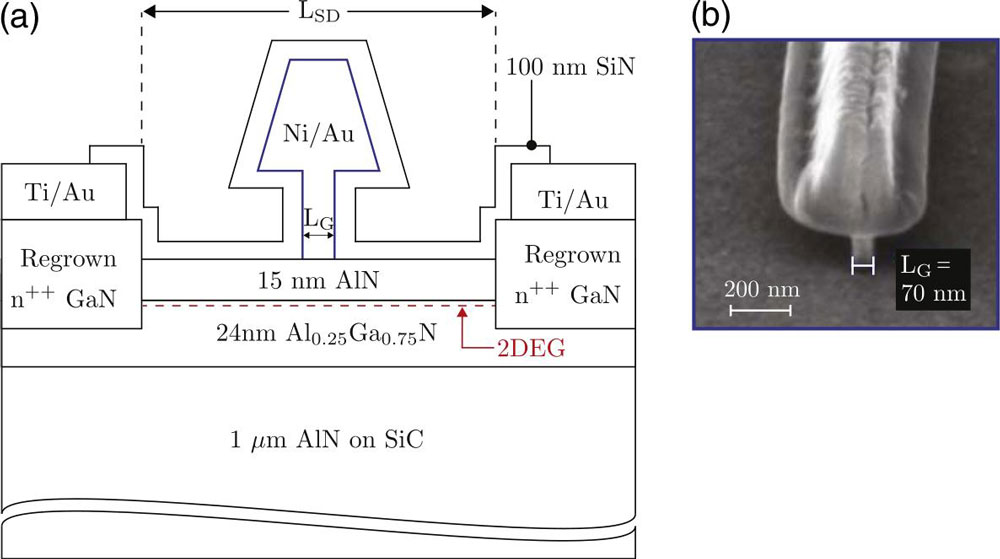
Figure 1: (a) Cross-sectional scheme of AlN/AlGaN/AlN HEMTs with T-shaped gate. (b) Scanning electron microscope (SEM) image of 70nm gate.
The gate consisted of 10nm nickel Schottky contact and 300nm gold, positioned mid-way between the source and drain. The gate length (LG) and width were 70nm and 2x25μm, respectively. The source−drain spacing (LSD) was 600nm.
The team reports: “The regrown n+ GaN non-alloyed ohmic contacts exhibited Rc = 0.23Ω-mm, which is the lowest contact resistance to 2DEG among all AlGaN-channel HEMTs reported in the literature.”
At 5V drain bias the device demonstrated 106 on/off current ratio and 0.11S/mm peak transconductance. The drain current density reached 0.9A/mm at 2V gate potential. The on-resistance (Ron) was 6.5Ω-mm.
The relatively thick AlN top barrier was thought to result in short-channel effects (SCEs), such as an output conductance higher than the Cornell group’s previous AlN/GaN/AlN QW HEMTs. The researchers believe these effects could be reduced by thinning the barrier, bringing the gate closer to the channel for improved electrostatic control.
Pulsed (500ns, 1kHz) operation showed current collapse/dispersion around 10%. The researchers comment: “The possible sources of current dispersion include the surface states and a formation of a two-dimensional hole gas or a filling of hole traps located near the valence band edge at the bottom GaN/AlN interface with a net negative polarization charge. To suppress RF dispersion in future devices, a proper control of surface states with an in-situ passivation layer and a Si-δ doping in the AlN back barrier to compensate positive charges may be necessary.”
Radio frequency measurements between 100MHz and 40GHz were used to calculate the fT and fmax frequency values.
The three-terminal breakdown was measured by subjecting the device to increasing drain bias (VDS) with the −10V gate potential below threshold, putting the device into its off state. Breakdown was considered to be when the off-current density exceeded 1mA/mm. The highest breakdown 59V was achieved in a device with 260nm gate-drain distance, giving an average breakdown field of more than 2MV/cm. However, on average 260nm LGD devices showed lower VBD values, reaching below 30V. Tests on a number of devices with 260nm, 370nm and 450nm LGD all had average breakdown fields greater than 1MV/cm. The good breakdown behavior offers potential for extremely high-power operation in RF applications with proper control of current-collapse-related dispersion.
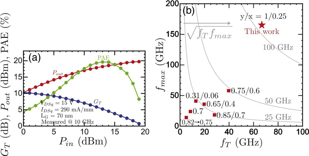
Figure 2: (a) RF power sweep at 10GHz at VDSq/VGSq = 15/−3V. (b) Benchmark comparing fT/ fmax of AlGaN-channel HEMTs reported in literature and Cornell’s latest work. y/x indicates the aluminium composition in the top barrier/channel layer (AlyGa1−yN/AlxGa1−xN).
The power capability was assessed using a Maury load-pull system at 10GHz (Figure 2). The power-added efficiency (PAE) and power density reached 20% and 2W/mm, respectively. The power gain (GT) was 5.2dB at 20% PAE. The researchers see the limitation on PAE and power output as being related to surface or bulk trap states.
The author Mike Cooke is a freelance technology journalist who has worked in the semiconductor and advanced technology sectors since 1997.


