


News: LEDs
11 May 2023
Record sub-micron LED red emission efficiency
University of Michigan in the USA claims record efficiencies from red-emitting sub-micrometer light-emitting diodes (LEDs) [Ayush Pandey et al, Appl. Phys. Lett., v122, p151103, 2023]. Some of the intellectual property arising from the work has been licensed to NS Nanotech Inc, co-founded by one of the paper’s authors, Zetian Mi. The company has in return funded some of the research.
Micron-scale LEDs are of particular interest for more efficient and versatile display technologies. The red sector of the visible part of the spectrum has been a particular roadblock, with conventional devices suffering poor performance in micron-scale form factors.
Although millimeter-scale III-nitride LEDs based on indium gallium nitride (InGaN) LEDs have very poor performance for red emission, the impact of scaling to the micron-scale is less marked, and in some respects offers enhanced operation compared with conventional devices.
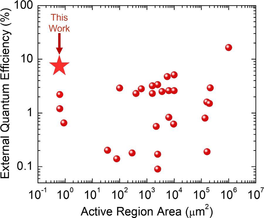
Figure 1: Variations of peak EQE with device active region area for reported red-emitting InGaN LEDs with emission peak more than 600nm.
The team reports (Figure 1): “By optimizing the p-type doping, a peak external quantum efficiency (EQE) of ~8.3% was measured for a sub-micrometer LED with an area of ~750x750nm2, which is the highest value reported for a red-emitting LED with lateral dimensions around 1μm, or less to our knowledge.”
The nanowires were formed by selective area growth (SAG) on N-polar GaN-on-sapphire templates, using a titanium mask (Figure 2). The team comments on the use of nanowire structuring: “The use of nanostructures offers several critical advantages, including significantly enhanced Mg dopant incorporation due to the efficient strain relaxation and the use of N-rich epitaxy conditions to suppress the formation of N-vacancy related defects.”
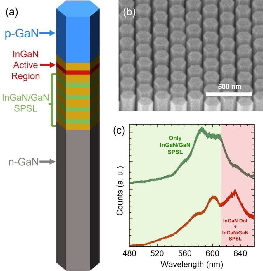
Figure 2: (a) Schematic of N-polar InGaN/GaN nanowire LED heterostructure. (b) Scanning electron microscope image of N-polar nanowire array. (c) Photoluminescence (PL) spectra of nanowires grown with and without InGaN dot, showing red emission from InGaN dot.
The initial ~500nm silicon-doped n-GaN layer was grown at 960°C. The strain-relaxer short-period superlattice (SPSL) consisted of four 8nm/8nm InGaN/GaN pairs, grown at a reduced temperature.
The 15nm active region consisted of high-indium-content InGaN, grown at a lower temperature than the SPSL. The researchers comment: “We have previously shown that such an InGaN active region exhibits compositional inhomogeneity due to the effects of composition pulling and the diffusion of indium during the growth of high-temperature layers.”
The final magnesium (Mg)-doped p-GaN layer was grown at a higher temperature than the active region. The tops of the nanowires were relatively flat, unlike in Ga-polar growth where the final p-GaN tends to have a rough surface, and other unwanted effects.
Red PL emission was achieved by adding an InGaN quantum dot section to the active region. The photoluminescence was multi-peaked due to indium content inhomogeneity and Fabry–Pérot interference effects between partially reflected light waves. Without the dot the dominant emission was in the green part of the visible spectrum.
Micro-LEDs were fabricated, beginning with 65nm atomic layer deposition (ALD) aluminium oxide for passivation and surface repair. Plasma-enhanced chemical vapor deposition (PECVD) silicon dioxide was added after etching back the passivation to expose the p-GaN of the nanowires. A 750nm x 750nm via was etched to give the micro-LED device area. The n-contact was titanium/gold. The p-contact consisted of nickel, gold and indium tin oxide (ITO) transparent conductor for current spreading.
The final step was application of a reflection layer to increase light emission from the sapphire substrate side of the device. The reflector consisted of silver, titanium, aluminium, nickel and gold layers.
The researchers compared devices with different Mg concentrations in the p-GaN layer of the nanowires, as measured by the beam-equivalent pressure supplied to the growth process. A high Mg concentration was given by a pressure of 5x10⁻⁸Torr, giving the material for device “A”. A non-optimized, low-Mg-content device “B” resulted from 5x10⁻⁹Torr pressure. Higher Mg concentrations than that used for device A tended to give “degradation of nanowire morphology”.
Device B showed its poorer performance in high current leakage in both forward and reverse bias, and hence lower light output. Device A achieved a peak external quantum efficiency (EQE) of 8.3% when the current density was 1A/cm2. The output power density at this point was 15mW/cm2, sufficient for display applications, according to the team. The light detector was mounted on the micro-LED with an index-matching fluid.
The researchers comment: “Typical high-efficiency organic LEDs, which have been adopted in displays, reach their peak efficiency at lower currents (of the mA/cm2 order), so the micro-LEDs described here would still have significantly improved brightness as compared to them.”
The team credits “improved hole injection into the device active region, relatively low electron overflow and reduced current leakage” for the improved performance of LED A.
The spectral output (Figure 3) of device A peaked at 650nm, deep red, for an injection of 0.5A/cm2. There is significant blue-shift, but the emissions remain in the red sector of the spectrum, greater than 600nm wavelength, up to 10A/cm2 injection.
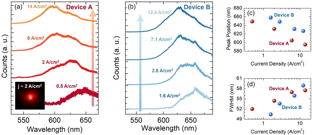
Figure 3: Electroluminescence (EL) spectra with various injection currents for devices (a) A and (b) B. Inset: (a) image of device under operation. (c) Peak position and (d) full-width at half-maximum (FWHM) versus current density.
The team comments: “The strong blue-shift at higher injection currents is likely a combination of the quantum-confined Stark effect (QCSE), as well as from the increased contribution of the SPSL in device emission. The QCSE can be potentially addressed through approaches such as strain engineering, polarization doping, or by creating an external optical cavity.”
The author Mike Cooke is a freelance technology journalist who has worked in the semiconductor and advanced technology sectors since 1997.


