


News: LEDs
4 May 2023
Thick single quantum well InGaN LEDs with high external quantum efficiency and low droop
University of California Santa Barbara in the USA and École Polytechnique in France have reported improved external quantum efficiency (EQE) and reduced efficiency droop in c-plane light-emitting diodes (LEDs) with thicker indium gallium nitride (InGaN) single quantum wells (SQW) [Y. C. Chow et al, J. Appl. Phys., v133, p143101, 2023].
The team used doped barriers to reduce the internal electric field in the well region. Such fields tend to separate holes and electrons, reducing radiative recombination into photons. Instead, the energy of the injected carriers is dissipated in non-radiative recombination processes: Shockley–Read–Hall (SRH) through recombination center defects at low injection, and Auger three-body interactions at high current and carrier density, creating (non-thermal) efficiency droop.
A thick QW would allow reduced Auger recombination for the same output — in theory. However, thin QWs are used for to bring the electrons and holes closer together, increasing their chances of recombining into photons.
The electric fields arise from charge polarization contrasts between the GaN and InGaN chemical bonds, resulting in polarization charges at the GaN/InGaN interfaces. Doped barriers would introduce a countervailing component to the electric field from the depletion of the doped regions, leaving ionized impurities. Another approach is to begin with non-polar or semi-polar substrates; however, these are much more expensive than the sapphire typically used to grow c-plane GaN/InGaN.
As usual, life is not straightforward. Doped material tends to have higher SRH-inducing defect densities. Hence, the research team performed a wide range of preparatory simulation and experimental work to find the right balance of parameters. Key ones were the doping concentration, and the separation of the doped regions from the quantum well.
The researchers grew a range of epitaxial LED structures on patterned sapphire substrates, using metal-organic chemical vapor deposition (Figure 1). The inner active region around the QW was varied in terms of acceptor and donor doping levels of the GaN barriers (NA and ND) and and the unintentionally doped (UID) GaN interlayer thicknesses (w1 and w2).
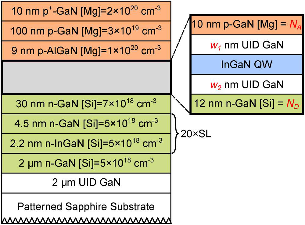
Figure 1: Schematic epitaxial LED structure.
After describing a number of experiments with such differences, the team comments: “In general, we found that the n-side UID interlayer is less important than the p-side UID interlayer, where the complete removal of the n-side UID interlayer is beneficial to the device performance of thick SQW LEDs. On the other hand, the optimized thickness of the p-side UID interlayers depended on the doping levels of the p-GaN doped barriers.”
The work resulted in two optimized devices with 7nm and 9nm SQWs with 16% and 13.5% indium content, respectively. The p-GaN was separated from the SQW by 2nm of UID GaN. The p- and n-type doping levels of the barriers were 1.7x and 1.5x10¹⁹/cm3, respectively.
The packaged devices included indium tin oxide (ITO) current-spreading layers, and dielectric omnidirectional reflectors. Apart from increasing the light emission from the back-side of the wafer, the reflectors served as metal insulation for the metal contacts. Sidewall passivation was provided by atomic layer deposition (ALD) silicon dioxide. The diced LED chips were wire-bonded and encapsulated in silicone.
The EQE was measured in an integrating sphere (Figure 2). Above 50A/cm2 current density, the injection was pulsed to avoid thermal effects. The shorter-wavelength ‘violet’ LED reached an EQE of 49% at 40A/cm2. The higher-indium-content, longer-wavelength ‘blue’ LED peaked at 39% EQE with 30A/cm2 injection. The devices peaked in EQE at current densities higher than the <10/cm2 typical of c-plane LEDs with thin QWs.
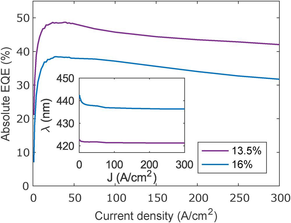
Figure 2: EQE versus current density of two thick SQW LEDs with doped barriers. Inset: EL peak wavelength versus current density.
The researchers comment: “The lower efficiency of the blue LED is likely related to poorer material quality and a higher piezoelectric field in the QW with a higher indium composition.”
The droop at 100A/cm2 was 6% and 3% for the violet and blue LEDs, respectively. The corresponding droops at 300A/cm2 were 14% and 17%. Thinner 3nm QW LEDs with similar peak EQEs tend to droop 40-60% by the time 300A/cm2 injection is reached.
The researchers comment: “The low efficiency droop of our devices can be attributed to a lower n [carrier density] as a result of a larger active region volume. These c-plane thick SQW LEDs also have comparable or better droop performance and peak EQE when compared to the non-polar and semi-polar LEDs reported in the literature. Nonetheless, they are still significantly lagging behind the state-of-the-art commercial c-plane LEDs in terms of the peak EQE (~80%).”
The blue-shifts of the violet and blue LEDs in going to higher current were 1.5nm and 6nm, respectively. The relatively small shifts suggest a lower quantum-confined Stark effect due to a lower electric field in the well. LEDs grown in the c-plane direction usually have shifts of more than 10nm.
The team writes: “There is less electric field to be screened by injected carriers, resulting in a smaller variation in wavelengths with respect to the current density.”
The author Mike Cooke is a freelance technology journalist who has worked in the semiconductor and advanced technology sectors since 1997.


