


News: Microelectronics
9 May 2023
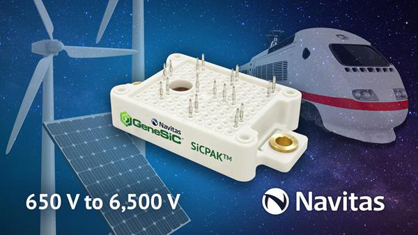
Navitas enters high-power markets with GeneSiC SiCPAK modules and bare die
Gallium nitride (GaN) power IC and silicon carbide (SiC) technology firm Navitas Semiconductor of Torrance, CA, USA has expanded its portfolio into higher-power markets with its silicon carbide power products in SiCPAK modules and bare die.
Target applications span centralized and string solar inverters, energy storage systems (ESS), industrial motion, electric vehicle (EV) on-board chargers, EV roadside fast chargers, wind energy, uninterruptible power system (UPS), bi-directional micro-grids, DC–DC converters, and solid-state circuit breakers.
Ranging from 650V to 6500V, Navitas claims to have the widest range of SiC technology. From an original line-up of discrete packages — from 8mm x 8mm surface-mount QFNs to through-hole TO-247s — the GeneSiC SiCPAK is an initial, direct entry point into higher-power applications. A comprehensive power module roadmap — with high-voltage SiC MOSFETs and MPS diodes, GaN power ICs, high-speed digital isolators and low-voltage silicon control ICs — is being mapped out.
“With a complete portfolio of leading-edge power, control and isolation technology, Navitas will enable customers to accelerate the transition from fossil fuels, and legacy silicon power products to new, renewable energy sources and next-generation semiconductors, with more powerful, more efficient, faster-charging systems,” says Dr Ranbir Singh, executive VP for SiC.
SiCPAK modules employ ‘press-fit’ technology to offer compact form factors for power circuits and deliver cost-effective, power-dense solutions to end users. The modules are built on GeneSiC die. Examples include a SiCPAK half-bridge module, rated at 6mΩ, 1200V, with trench-assisted planar-gate SiC MOSFET technology. Multiple configurations of SiC MOSFETs and MPS diodes will be available to create application-specific modules. The initial release will include 1200V-rated half-bridge modules in 6mΩ, 12mΩ, 20mΩ and 30mΩ ratings.
Within the lead-free SiCPAK, each SiC chip is silver (Ag) sintered to the module’s substrate for superior cooling and reliability. The substrate itself is ‘direct-bonded copper’ (DBC) and manufactured using an active-metal brazing (AMB) technique on silicon nitride (Si3N4) ceramics, suitable for power-cycling applications. This construction delivers what is claimed to be excellent strength and flexibility, fracture resistance, and good thermal conductivity for cool, reliable, long-life operation.
For customers who prefer to make their own high-power modules, all GeneSiC MOSFET and MPS diodes are available in bare die format, with gold (Au) and aluminium (Al) top-side metalizations. Parts are available now to qualified customers.


