


News: Optoelectronics
18 May 2023
All-MOCVD 980nm laser on (001) silicon
Hong Kong University of Science and Technology and the Chinese University of Hong Kong have reported continuous wave (CW) 980nm laser operation from structures grown on silicon (Si) by metal-organic chemical vapor deposition (MOCVD) [Qi Lin et al, Optics Express, v31, p15326, 2023]. The team used indium gallium arsenide phosphide (InGaAsP) layers for the quantum wells (QWs), and aluminium gallium arsenide (AlGaAs) for the barriers and cladding.
The researchers see the 980nm wavelength as having potential for optical fiber communication and internet protocol network systems. In particular, 980nm light can be used to pump erbium-doped fiber amplifiers (EDFAs).
The laser structure (Figure 1) was grown on (001) silicon, as used in mainstream complementary metal-oxide-semiconductor (CMOS) electronics manufacturing. The epitaxial growth was through MOCVD in two reaction chambers for the GaAs template and for the laser structure.
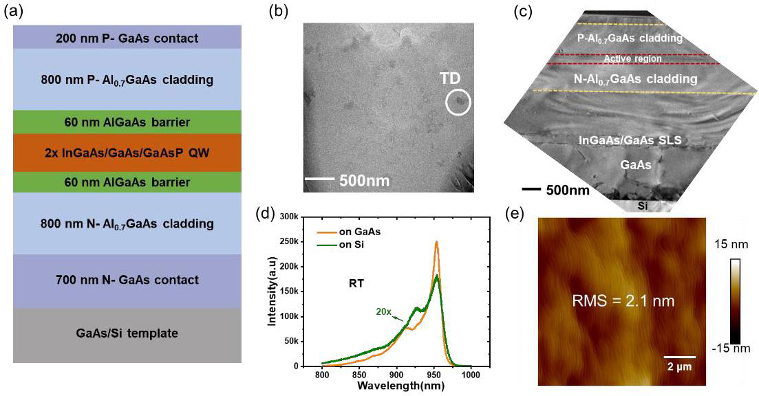
Figure 1: (a) Schematic of 980nm InGaAs/GaAs/GaAsP QW laser grown on GaAs/Si template; (b) Plan-view transmission electron microscope (TEM) images of 2μm-thick GaAs/Si template; (c) Global view cross-sectional TEM image of laser structure; (d) Room temperature (RT) μ-photoluminescence (PL) of structure; (e) Atomic force microscope image.
The first growth was of the GaAs template layer, which included InGaAs/GaAs strained-layer superlattices (SLSs) to filter threading dislocations (TDs). Thermal cyclic annealing (TCA) was carried out before the SLS to improve the quality of the initial 1μm GaAs layer. The complete template layer was 2μm thick with the 2.8x10⁷/cm2 TD density.
The laser structure was grown in the second reaction chamber with strain-compensated InGaAs/GaAs/GaAsP quantum wells. The PL emission peak was at 956nm. A reference structure grown on GaAs substrate had a PL peak at the same wavelength.
The epitaxial material was fabricated into ridge-waveguide edge-emitting laser diodes (LDs). The n- and p-electrodes were titanium/platinum/gold and germanium/gold/nickel/gold, respectively. Passivation was provided by silicon dioxide. The material was thinned to 100μm and cleaved into laser bars without facet coatings. The CW measurements were made with the laser diodes mounted on temperature-controlled heatsinks.
The lowest lasing threshold current, 40mA, was achieved on a 2μmx1mm laser diode (Figure 2). The lowest threshold current density was 938A/cm2 on a 40μmx1.2mm laser diode. This compares with a reference 70μmx2mm device on GaAs that demonstrated a lower 179A/cm2 threshold.
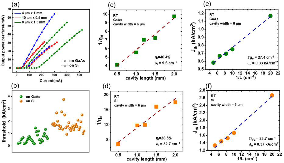
Figure 2: (a) Output power-current curves of InGaAs/GaAs/GaAsP QW lasers with various cavity size grown on GaAs and silicon; (b) threshold density distribution; extractions of (c) (d) internal quantum efficiency (IQE ηi), internal loss (αi), (e) (f) modal gain (Γg0) and transparency current density (Jtr), from cavity-length-dependent measurement.
The CW threshold on silicon is a little higher than the 867A/cm2 reported last year (see Semiconductor Today news, 2022) for a 980nm laser diode on silicon grown by MOCVD (GaAs template) and molecular beam epitaxy (laser) at Beijing University of Posts and Telecommunications. The Beijing device was pretty short-lived at 12 minutes. The Hong Kong team does not report on the endurance of its laser diodes, although the Beijing life-time is considered “unacceptably short”.
The team comments: “Initial results show that the average threshold current density of the ridge-waveguide lasers on silicon (~1.91kA/cm2), is approximately five times higher than devices on the native GaAs substrate (~410A/cm2).”
The single-facet output power reached 46.4mW on silicon, compared with 65mW on GaAs substrate.
The greater spread in threshold current density and other laser diode performance limitations on silicon are tentatively attributed to the poorer quality of the GaAs template layer in comparison with what is achievable on native GaAs substrates. The poorer-quality template layer affects the QW uniformity, for example.
The researchers comment: “Based on the investigation of the internal parameters, a better laser performance with lower non-radiative losses can be achieved by further reducing the defects density of the GaAs film grown on silicon substrate via additional dislocation reduction approaches. In addition, laser performance improvement could also be achieved by enhancing the quality of QWs through optimization of parameters including the QW thickness and indium composition.”
The laser diodes on silicon were capable of lasing beyond the 95°C limit of the measurement equipment. The characteristic temperature (T0) scale for the shift to higher thresholds was 71.8K, average. The T0 for the reference devices on native GaAs was 139.1K. The maximum values were 157K (10μmx0.5mm) and 84K (2μmx1.5mm) for laser diodes on GaAs and silicon, respectively.
https://doi.org/10.1364/OE.484831
www.semiconductor-today.com/news_items/2022/sep/beijinguni-010922.shtml
The author Mike Cooke is a freelance technology journalist who has worked in the semiconductor and advanced technology sectors since 1997.


