


News: LEDs
2 March 2023
Green exciton emission from nanowire micro-LEDs
University of Michigan in the USA reports high-efficiency green emission from micron-scale light-emitting diodes (LEDs) using bottom-up growth of nanowires, allowing strain and quantum engineering [Ayush Pandey et al, Nano Letters, published online 2 February 2023].
The researchers claim record peak external quantum efficiency (EQE) and wall-plug efficiency (WPE), compared with devices with a similar active region area. Such devices are being developed for next-generation displays, virtual/augmented reality, and ultrahigh-speed optical interconnects.
The Michigan researchers believe that the higher efficiencies are due to excitonic, rather than free electron-hole, recombination.
The team explains: “In an excitonic LED, electroluminescence emission originates from a bound state of an electron and hole, instead of recombination from free charge carriers. Due to the strong Coulombic interaction between electrons and holes, the negative impact of Shockley–Read–Hall recombination on the performance of an excitonic LED is significantly reduced.”
In conventional indium gallium nitride (InGaN) LEDs excitonic recombination is hindered by the presence of strong electric fields arising from strain-dependent and spontaneous charge-polarization contrasts of InGaN and GaN. The electric fields tend to tear apart electron–hole excitons, and further even reduce the ability of free holes and electrons to recombine into photons. These behaviors are referred to as the quantum-confined Stark effect (QCSE).
Further optimization may be possible in terms of the strain state, composition and thickness of the InGaN active region in the nanowires along with the dimensions of the nanowires themselves. The team suggests that “micro-LEDs with emission across the entire visible spectrum could be grown, with efficiencies approaching to, or better than, commercial broad-area LEDs.”
To grow the nanowires, the Michigan researchers first patterned a titanium mask on an N-polar GaN-on-sapphire template using electron-beam lithography. The titanium was opened to expose the underlying GaN by reactive-ion etching. Before nanowire growth, the mask surface was nitrided with nitrogen plasma exposure.
Comprising n-GaN, active region, and p-GaN (Figure 1), the nanowires were grown via molecular beam epitaxy (MBE). The active region was grown at lower temperature than the two contact layers. Also, the researchers targeted green emission from the InGaN layers of the active region with an In/Ga flux ratio of 0.6. The active region consisted of 6 pairs of InGaN/GaN multiple quantum disks (MQDs).
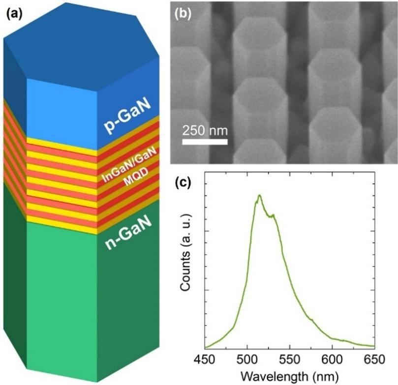
Figure 1: (a) Schematic of N-polar InGaN/GaN nanowire excitonic LED heterostructure. (b) Representative scanning electron microscope (SEM) image of nanowire array. (c) Photoluminescence (PL) spectrum of nanowire array.
The growth resulted in hexagonal vertical nanowires with flat tops, which are desired for the fabrication of high-efficiency devices. Ga-polar nanowire growth tends to result in tapered structures. Also, the growth of nanowires from the bottom up avoids the sidewall damage of top-down methods where the nanowires are formed from etching standard materials.
The photoluminescence from the material peaked in the green region of the spectrum. The peak was quite broad with some shoulders, which the researchers attribute to “Fabry–Perot modes formed with the substrate”.
The team comments: “The luminescence spectrum is relatively broad, due to variations in indium composition of the quantum disks”.
Analysis using scanning transmission electron microscopy and x-ray energy-dispersive element mapping suggested ‘faceting’ near the sidewalls of the nanowires. This refers to preferred growth of the layer parallel to semi-polar planes rather than the c-plane. One result was higher indium incorporation near the sidewall. Also, it is to be expected that there is reduced strain in the semi-polar faceted regions, resulting in reduced QCSE and hence tighter exciton binding. Faceting was more prominent in smaller-diameter nanowires, around 125nm (array/device A) compared with 165nm (B).
Micro-LEDs were fabricated by atomic layer deposition (ALD) of 65nm aluminium oxide coating the nanowires; etching back to expose the p-GaN contact layer; plasma-enhanced chemical vapor deposition (PECVD) of 500nm silicon dioxide insulation; and etching of vias for deposition of the metal n- and p-type electrodes.
The n-electrodes were titanium/gold, while p-electrodes were nickel/gold/indium tin oxide (ITO). The light emission was arranged through the sapphire backside by coating the top side with a mirror consisting of silver/titanium/aluminium/nickel/gold.
The micro-LED devices were prepared for testing by thinning the sapphire backside, and dicing into small pieces. The current injection area was around 750nmx750nm.
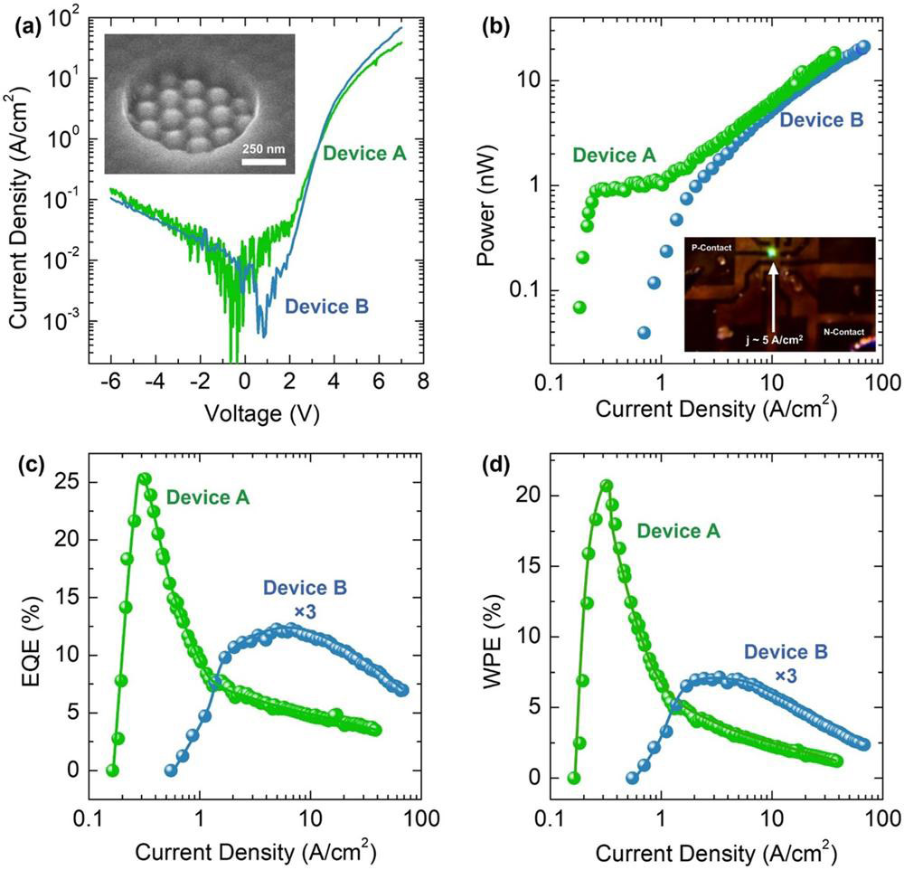
Figure 2: (a) Current density versus voltage. Inset: SEM image of representative injection opening. (b) Light output power versus current density. Inset: image of strong green emission from submicron device. (c) External quantum efficiency (EQE) and (d) wall-plug efficiency (WPE) versus current density.
Device A with narrower nanowires exhibits better performance overall (Figure 2). The peak in the efficiencies comes sooner (around 0.3A/cm2) however, before fall off at higher current injection. The peak EQE and WPE for device A were 25.2% and 20.7%, respectively. The researchers comment that these efficiencies are “significantly higher than conventional quantum well micro-LEDs of similar dimensions”. The high WPE also indicates excellent carrier conduction in the device, particularly with respect to hole injection into the active region.
The team points out: “While the efficiency peak occurs at low current, corresponding to low absolute output power, the small size of an individual device allows several of them to be arranged in larger arrays, greatly boosting their total power for applications that demand it.”
The 4.1% EQE peak for device B came at 5A/cm2. The researchers suggest that the efficiency droop at higher injection could be reduced by including an electron-blocking layer between the active and p-contact regions.
The power output of device A has a fast rise at low current, then the power saturates before rising again more slowly, in line with the performance of device B with wider nanowires. The researchers attribute this behavior to indium-rich clusters in the faceted region of the quantum disks dominating the emissions at low injection, “due to their higher indium compositions and proximity to the highly doped nanowire sidewalls”.
At higher injection, the clusters are saturated and emission increases of the MQDs must come from the more central c-plane portions with free electron–hole recombination, instead of excitons.
These behaviors were also clarified by spectral analyses: at low current there was a dominant ‘green’ peak in device A, around 515nm wavelength. As the current injection increased, higher-energy emissions from shorter, bluer wavelengths in the 475–490nm range came to dominance. The spectral behavior of device B showed only dominance of emission from free electron–hole recombination. Device B, and device A with injection above a few A/cm2, show operation corresponding to conventional quantum well LEDs, according to the researchers.
The author Mike Cooke is a freelance technology journalist who has worked in the semiconductor and advanced technology sectors since 1997.


