


News: Microelectronics
23 March 2023
GaN on silicon through surface-activated bonding
Researchers from UK, China and Japan have been exploring the potential of surface-activated bonding (SAB) as a means to create high-quality gallium nitride (GaN) on silicon (Si) with a view to low-cost, large-scale and multi-functional GaN/Si device applications [Yan Zhou et al, Appl. Phys. Lett., v122, p082103, 2023].
The technique avoids thick aluminium gallium nitride (AlGaN) heterostructures of direct GaN growth on silicon. Such layers are needed to bridge the large 17% lattice mismatch between GaN and silicon generating performance-sapping dislocations and other defects. The main attraction of using GaN/Si — rather than better matched silicon carbide, diamond or free-standing GaN substrates — is cost.
The drawback for applications — particularly ones involving heat generation such as for high-power/voltage management, for which there is much interest in GaN-based devices — is that these layers tend to be thermally resistive. This makes thermal management much more difficult.
The team — from University of Bristol in the UK; State Key Laboratory of Superlattices and Microstructures, University of Science and Technology of China, Center for High Pressure Science and Technology of Advanced Research, and Harbin Institute of Technology, Beijing University of Technology in China; and Osaka City University and Osaka Metropolitan University in Japan — also found that annealing could convert the relatively thick amorphous layer of the bond formed at room temperature to a much thinner crystalline layer.
The epitaxial GaN was grown on 4-inch n-Si(111) wafers using metal-organic chemical vapor deposition (MOCVD) with trimethyl-Ga/Al and ammonia (NH3) precursors. The 1.2μm 1000°C GaN layer was grown on 200nm 1060°C AlN buffer.
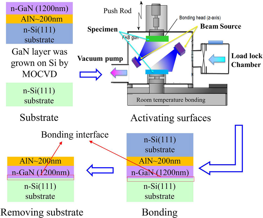
Figure 1: Schematic SAB process to fabricate GaN/Si heterostructure.
The surface activation (Figure 1) for the bonding consisted of fast argon atom beam irradiation of both the target n-Si(111) wafer and the epitaxial GaN/Si wafer. The bonding was carried out at room temperature in 7x10⁻⁷Pa vacuum with 1GPa external load for a minute.
The silicon epitaxial growth wafer was removed by chemical polishing and wet etching. The target wafer was protected from the etching by RF-sputtered silicon dioxide (SiO2). Epitaxial growth produced Ga-polar GaN, and therefore the GaN/Si target wafer-bonded material was N-polar.
The stress state of the GaN/Si was studied using Raman spectroscopy. The researchers estimated a residual stress of 0±005GPa by comparing the E2high Raman peak shift relative to free-standing GaN grown by hydride vapor phase epitaxy (HVPE), assumed stress-free. This compares with MOCVD GaN/Si-grown samples, which had typical values of −0.05±0.09GaP (compressive) stress.
The team also studied the stress after annealing the SAB samples at 400°C, 700°C or 1000°C for 300s in nitrogen atmosphere. At the highest annealing temperature, a tensile stress of 0.16GPa developed, but at the lower temperatures the stress was negligible.
Transmission electron microscope (TEM) examination of the interface before and after 1000°C annealing showed the effect of the thermal process to be the transformation of an amorphous layer into a thin crystallized interlayer (Figure 2). The amorphous bond layer was of the order of tens of nanometers, while the crystallized interlayer was only a few nanometers. The inspection also found that “no structural defects, such as cracks, were observed at the interface whether without or with annealing.”
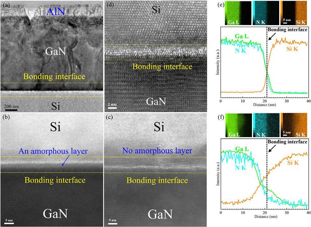
Figure 2: Low (a) and high-magnification (b) cross-sectional TEM images of GaN/Si bonding interface fabricated by SAB without annealing. High-magnification (c) and high-resolution (d) cross-sectional TEM images of bonding interface after annealing at 1000°C. EDS mapping of bonded interface region (e) without annealing and (f) after annealing at 1000°C.
According to energy-dispersive x-ray spectroscopy (EDS) mapping, the crystallized interlayer consisted of Ga, N and Si. There was also some diffusion of these elements into the neighboring GaN/Si materials.
The researchers attribute the amorphous layer of the unannealed samples to the effect of the surface activation in the bonding process, creating a cushion and allowing the GaN to relax over the silicon target wafer, despite the 17% lattice mismatch.
The researchers suggest that their study indicates that “it is possible to obtain stress-free GaN epitaxial layers through SAB technique at room temperature and tune the interlayer structure and residual stress through appropriate temperature annealing.”
The author Mike Cooke is a freelance technology journalist who has worked in the semiconductor and advanced technology sectors since 1997.


