


News: Optoelectronics
15 June 2023
Co-doping boost for quantum dot lasers on Si(001)
China’s Key Laboratory of Semiconductor Materials Science and the University of Chinese Academy of Sciences claim significantly enhanced performance of indium arsenide (InAs) quantum dot (QD) lasers on silicon (Si) by spatially separated co-doping [Shuai Wang et al, Optics Express, v31, p20449, 2023].
The researchers attribute much of the improved performance as being due to “effective passivation of non-radiative recombination centers around the QDs by n-type direct doping” in the active light-generating region of the device (Figure 1). This region consisted of a stack of five indium gallium arsenide (InGaAs) wells separated by p-doped (beryllium) GaAs barriers. The InAs QDs were grown in the wells doped with silicon at 4.4x10¹⁰ dots/cm2 density.
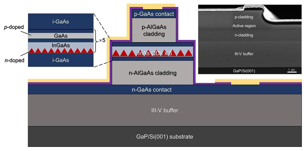
Figure 1: Silicon-based InAs/GaAs QD laser structure. Top-left inset: schematic of separated co-doping in QD active region; top-right: scanning electron microscope (SEM) image of front facet.
The researchers comment on the effect of n-doping the QDs: “The carrier loss is reduced and the mode gain of the QD lasers is improved especially for the situation under high injection current and operating temperature.”
Previously, modulation p-doping of the barriers in QD lasers has been found effective in compensating for hole loss during device operation, resulting in improved differential gain, temperature stability, and small-signal modulation response. However, one drawback is an increased threshold current due to higher non-radiative Auger recombination rates, negatively impacting power consumption.
Doping the QDs n-type has resulted in lower threshold current density, higher slope efficiency, smaller linewidth enhancement factor, and a narrower near-field lasing spot. Co-doping with p-type barriers and n-type dots has been shown to reduce power consumption and improve thermal stability. Deploying the co-doping technique on silicon substrates has the potential to compensate for the reduced material quality (increased defects) of III-V epitaxial layers.
The researchers comment: “This work shows the great promise of co-doping technique for enhancing silicon-based QD laser performances towards lower power consumption, higher temperature stability, and higher operating temperature, to boost the development of future low-cost and high-performance silicon photonic chips.”
The laser material structure was grown by solid-state molecular beam epitaxy (MBE) on gallium phosphide (GaP) on Si(001) templates with a view to avoiding anti-phase boundary defects.
The 2700nm III-V buffer consisted of 1600nm GaAs, 200nm dislocation filter (DFL), and 900nm GaAs spacer layer. The DFL contained ten groups of superlattice strain layers (10nm In0.14Ga0.86As/10nm GaAs). Cyclic annealing improved the crystal structure. The threading dislocation density was estimated as being as low as 8.7x10⁶/cm2.
The waveguide layers were GaAs, and the cladding was aluminium gallium arsenide (Al0.4Ga0.6As).
A reference material was also grown without n-doping of the QDs. The doping concentrations were around 1x10¹⁸/cm3. For the barrier p-type doping this corresponded to about 13.6 holes/dot; for the smaller volume of dots, the doping gave around 1.6 electrons/dot, it is estimated.
The epitaxial materials were fabricated into standard 6μmx1mm ridge-waveguide laser diodes (LDs). The cleaved facets were coated with 97% reflective dielectric stacks consisting of silicon dioxide and tantalum pentoxide (SiO2/Ta2O5) layers.
The p+n co-doped QD laser achieved a threshold current of 28.1mA (468A/cm2) in continuous wave (CW) operation at room temperature (25°C). The p-only diode had a 40.3mA (672A/cm2) threshold. Other reported p-only QD laser diodes have reached thresholds as low as 266A/cm2, suggesting room for improvements and optimizations.
The maximum power output reached 69mW in the co-doped laser diode, while the p-only device reached 55mW. The saturation currents were 375mA and 335mA, respectively. The slope efficiency of both devices was around 0.27W/A below 200mA injection.
The ground-state laser wavelengths were 1305nm (at 40mA) and 1296nm (50mA) for the n+p and p-only doped laser diodes, respectively.
The thermal performance of the laser diodes was assessed in pulsed mode between 15°C and 115°C. At the highest temperature, the co-doped device had a 102mA threshold, compared with 267mA for the p-only laser diode. The maximum power output from the co-doped diode was 8mW at 115°C. The characteristic temperatures for the thresholds (T0), 15-85°C, were 102K and 87K for the co-doped and p-only devices, respectively. The corresponding characteristics for the slope efficiency (T1), 15-55°C, were 556K and 513K.
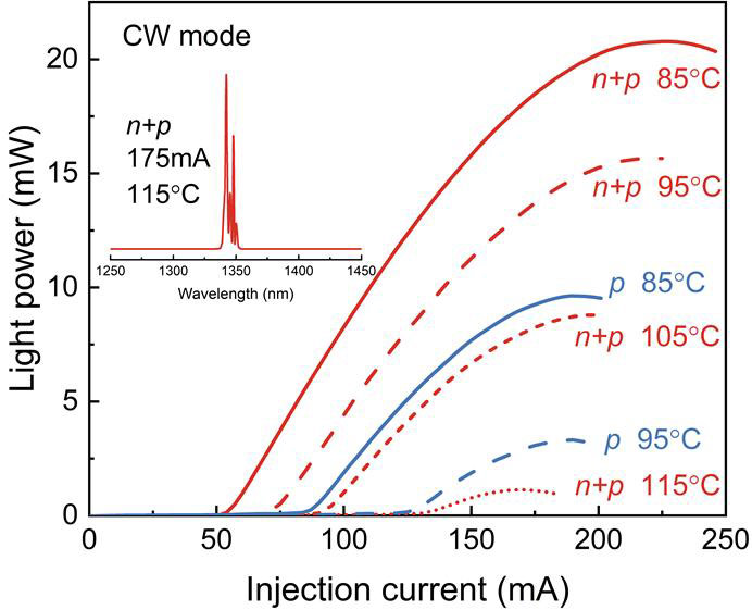
Figure 2: CW light output power–current curves of p-doped alone and co-doped QD lasers above 85°C. Inset: optical spectrum of co-doped laser under 175mA CW current.
The researchers report that the n+p laser diode maintained ground-state lasing with a peak wavelength of about 1342.2nm under 175mA CW operation at 115°C (Figure 2), adding: “To the best of our knowledge, this result is better than the highest CW operating temperature reported so far for p-doped alone QD lasers grown on Si(001) of 108°C and is close to the best value on offcut silicon (not CMOS compatible) of 119°C.”
The team expects improvements from optimized material quality, doping concentrations, device processes, and packaging techniques.
The author Mike Cooke is a freelance technology journalist who has worked in the semiconductor and advanced technology sectors since 1997.


