


News: Optoelectronics
22 June 2023
Monolithic integration of III-V lasers and silicon photonics
Researchers based in France, Italy and Ireland claim the first demonstration of III-V semiconductor lasers grown on a patterned silicon photonics platform with light coupled into a waveguide [Andres Remis et al, Light: Science & Applications, v12, p150, 2023].
The team from University of Montpellier in France, Polytechnic University of Bari in Italy, and Tyndall National Institute and Munster Technological University, both in Ireland, report a butt-coupling efficiency of about 10% and an upper value for the insertion loss of 10dB. The gallium antimonide (GaSb)-based lasers emitted at a wavelength around 2.3μm. Such wavelengths have applications that include trace-gas sensing and the light-version of radar, LIDAR.
The researchers are seeking to overcome the roadblock for monolithic integration of lasers with low-cost, large-scale, fully integrated photonic integrated circuit (PIC) chips. The alternative approach is heterogeneously integrating separately-grown III-V epitaxial material, using wafer bonding techniques. The team comments: “Note that a recent comparison of epitaxial and heterogeneously integrated GaSb-based lasers revealed superior performances of epitaxial lasers in terms of threshold current density and maximum operating temperature. We thus expect the same to be true for the lasers studied here that are grown on a PIC.”
The group also hopes that the techniques used “can be extended to any semiconductor materials system provided the anti-phase domain problem can be solved, which is the case with most III–V systems nowadays, and the various processing steps are established, which does not pose fundamental issues.” Further, the availability of 300mm epitaxy systems raises the prospect for scaling up to large-diameter silicon wafer sizes and mass production of low-cost laser-powered PICs.
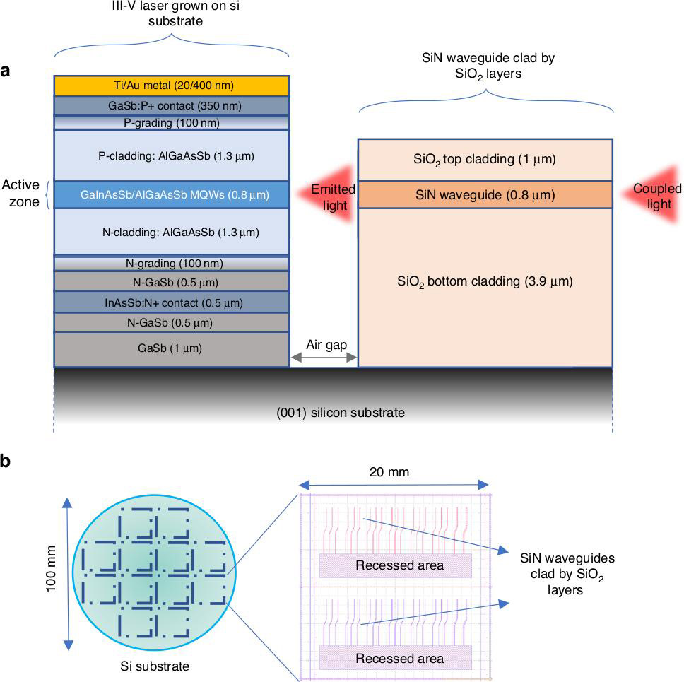
Figure 1: a Final device cross-section. b Schematic of silicon photonics PICs.
The platform for the silicon PICs consisted of silicon nitride (SiN) sandwiched between silicon dioxide (SiO2) cladding (Figure 1), processed at Tyndall National Institute in Ireland. The substrate was 100mm-diameter silicon. The bottom cladding was achieved through thermal oxidation of the substrate, and the top by plasma-enhanced chemical vapor deposition (PECVD).
The wafer was then patterned and etched to produce a series of waveguides with 300μm S-bend offset and 16mmx2.5mm recessed areas where the GaSb lasers were to be grown and fabricated. The researchers took extra care for the recess etching so that the III-V growth surface was not damaged by the etching. About 95% of the etching was by reactive-ion etch, but the last 5% was carried out by a slower hydrofluoric acid wet etch.
The researchers explain: “A one-step dry etch would have invariably damaged the silicon surface. In contrast, hydrofluoric acid wet etching being isotropic, wet etching of the entire thickness of the stack would have resulted in a concave dielectric facet.”
For the III-V epitaxy, the group used its previous work to avoid anti-phase boundary (APB) defects, burying them in the 1μm GaSb buffer layer. The buffer was grown in two steps on 20mmx20mm dies from the patterned PIC wafer by solid-source molecular beam expitaxy (MBE): 50nm at 400°C and the remainder at 500°C. Before the growth, native oxide was removed from the silicon surface by vacuum annealing in the MBE chamber at 1000°C. While the buffer was being grown, the researchers periodically inspected the materials to ensure an APB-free GaSb surface while preserving the silicon PIC integrity.
The laser structure itself was grown in a separate MBE reactor. The active region consisted of two gallium indium arsenide antimonide (GaInAsSb) quantum wells (QWs) confined by aluminium gallium arsenide antimonide (AlGaAsSb) barriers. The researchers estimate the threading dislocation density in the laser material at the order of 107/cm2. The root-mean-square surface roughness was as low as 2.5nm, according to atomic force microscopy (AFM).
Device fabrication began with removal of polycrystalline III-V residue deposited on the PIC dielectrics during MBE by a wet etch, involving citric and hydrofluoric acids, hydrogen peroxide, and water. The single-crystal laser material was coated with photoresist to protect it during this etch processing. The laser material was then fabricated into ridge-waveguide laser diodes. The facets were formed by etching rather than cleaving.
Each 20mmx20mm die was cleaved into two chips for testing. The chips contained eight laser diodes with 10μmx1.5mm ridges. The air gap between the laser facet and waveguides was around 15μm.
The turn-on voltage for the lasers was around 1V with various threshold currents in the range 135-150mA in continuous wave operation at room temperature. The series resistance was around 3Ω. The output power from the back facet at 400mA injection was in the range 7-10mW. Away from room temperature, the threshold for one device increased from 163mA to 283mA between 20°C and 80°C. The characteristic temperature for this increase (T0) was 110K. The researchers see these results as consistent with other reports of GaSb laser diodes on silicon.
The researchers then tested the butt-coupling of the laser light into the appropriate 10μm-wide waveguide (Figure 2). The coupling efficiency was about 10%. Since such waveguides typically have a low propagation loss of 0.1–2.5 dB/cm in the wavelength range of the laser light, the researchers consider most of the power loss between the source laser and detection at the end of the waveguide to be insertion loss from the butt-coupling. “We thus conclude that the upper value for the insertion losses in our system is 10dB,” the team reports.
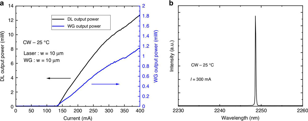
Figure 2: a Light output powers versus current for back facet of laser diode (black, left scale) and from waveguide (blue, right scale). b Emission spectrum recorded from laser diode at room temperature, CW operation, at ~2x threshold current.
The insertion loss could be improved by reducing the air-gap between the laser and waveguide to less than 2μm, according to simulations. Unfortunately, the team does not believe the gap can be reduced below 3μm, due to fabrication considerations.
An alternative approach could be to fill the gap with a material with a higher refractive index (n) than air (n = 1). The researchers comment: “Filling the gap with amorphous silicon (n = 3.44) or chalcogenide materials (n ~ 2.5) would allow a coupling efficiency higher than 50%, but filling a narrow gap with these materials might prove cumbersome. In contrast, filling the gap with polymers such as PMMA or BCB (n~1.5), which is easy to do given their liquid state before polymerization, would already give a coupling efficiency as high as 40%.”
The author Mike Cooke is a freelance technology journalist who has worked in the semiconductor and advanced technology sectors since 1997.


