


News: Optoelectronics
2 June 2023
GeSn VCSE p-i-n diodes bonded on 200mm silicon wafers
Researchers based in Singapore, the USA and China claim the “first demonstration” of 200mm (8-inch) wafer-scale germanium tin (GeSn) multiple-quantum-well (MQW) vertical-cavity-surface-emitting (VCSE) p-i-n structures and diodes [Qimiao Chen et al, ACS Photonics, published online 8 May 2023]. The team from Singapore’s Nanyang Technological University and National University of Singapore, China’s State Key Laboratory of Superlattices and Microstructures, and Applied Materials Inc in the USA, see the achievements as setting the stage for “laser or light-emitting diode (LED) applications in silicon photonics by wafer bonding and layer transfer techniques”.
The researchers also believe that the devices could be easily scaled up to production of 300mm (12-inch) wafers, since the MQW was grown on 300mm silicon (Si) substrates. VCSE lasers (VCSELs) are widely used as compact size devices with circular emission profile, low beam divergence, high bandwidth, and high coupling efficiency to fiber-optic cables. Fabrication is compatible with mass manufacturing using wafer-scale techniques.
Further, such devices being fabricated on silicon potentially opens the way to optoelectronic Nirvana, combining mainstream complementary metal-oxide-semiconductor (CMOS) electronics and laser light transmitted by silicon waveguides.
But we’re not there yet. Group IV alloys like GeSn have indirect bandgaps without some serious massaging. Materials with indirect bandgaps generally have low potential for light emission. In the case of GeSn the narrowest energy gap is between what are called L valleys placed at non-zero quasi-momentum in the conduction band down to the heavy-hole band with a peak at zero quasi-momentum. There are four such L valleys. The direct Γ valley (zero quasi-momentum) has a larger energy gap. The photon has effectively zero momentum, and electron−hole transitions to a photon, requires near zero change in quasi-momentum.
The difference between the gaps can be altered by (tensile) strain and band-filling. Thermal fluctuations can also increase the density of electrons in the Γ valley.
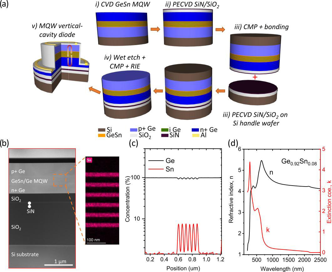
Figure 1. (a) Fabrication flow of GeSn/Ge MQW vertical-cavity surface-emitting structures and diodes on Ge-on-insulator (GOI) substrate. (b) Cross-sectional TEM with EDX mapping and (c) EDX line scan. (d) Optical constants from spectral ellipsometry.
The MQW structures were grown using reduced-pressure chemical vapor deposition (RPCVD). Ge0.92Sn0.08/Ge wells/barriers were grown on a 1μm Ge buffer and 470nm p+-Ge contact layers (Figure 1). The precursors were di-germane (Ge2H6) and tin tetrachloride (SnCl4). The structure was finished off with a 330nm n+-Ge contact layer.
The well thicknesses were kept below critical, so the growth was ‘pseudomorphic’ — i.e. the strain (−1.6%) did not relax through generation of misfits or threading dislocations. With this compressive strain the GeSn was still nominally indirect, with a calculated bandgap between the L valleys and the heavy-hole band of 549meV. Direct transitions from the Γ valley would release an energy 604meV, hopefully to a photon. As the L valleys fill with carrier injection, one expects thermionic effects to allow more electrons to be excited into the Γ valley, and some light to be emitted. Such excitation increases with temperature — at room temperature the thermal energy scale is around 26meV (Boltzmann’s constant x 300K), about half the gap between the L and Γ valleys.
The researchers comment: “It can be anticipated that further increasing Sn content in GeSn QW, relaxing the compressive strain or incorporating Si and Sn into the barrier layer can increase the directness of GeSn QW and carrier confinement in the GeSn QW. It thereby can further increase the optical gain due to more electrons occupied in Γ valley so as to achieve population inversion with reduced injection current densities.”
A 6-period MQW structure with 21nm wells separated by 32nm barriers was bonded to a 200mm silicon handle wafer. The 300mm donor wafer was prepared by dicing to 200mm, and plasma-enhanced chemical vapor deposition (PECVD) of 1486nm silicon dioxide (SiO2) and 27nm silicon nitride (SiN). The final handle wafer was also prepared with 27nm SiN and 287nm SiO2.
The bonding was at room temperature, followed by 300°C annealing in nitrogen atmosphere for 4 hours. The donor wafer and Ge buffer layers were removed by tetramethylammonium hydroxide (TMAH) etching, chemical mechanical polishing (CMP) and reactive-ion etching (RIE).
The SiO2/SiN dielectric bonding layers also served as a bottom reflector of the vertical-cavity structure.
Transmission electron microscopy (TEM) with energy-dispersive x-ray (EDX) mapping suggested the VCSE structures had a cavity length of 1083nm. Photoluminescence studies of the VCSE structure showed stronger emission relative to reference MQWs on the donor wafer. Also, the main peak of the VCSE came at 2148nm, which is 171nm longer than for the reference emissions.
The researchers comment: “Since the VCSE structure and reference samples have the same GeSn/Ge MQW structure, the difference is more likely due to the vertical micro-cavity effect rather than quantum-confined effect.”
The maximum PL enhancement of the VCSE structure over the reference was more than 8x at 2177nm. Simulations suggested that the MQWs were at an anti-node of the optical field in the Fabry−Pérot cavity.
The team comments: “Based on the simulation, the active GeSn/Ge MQW layer is spatially and spectrally aligned with the single-longitudinal-mode cavity of the MQW VCSE structure, which is the reason for the enhancement of the light emission from the MQW VCSE structure.”
The PL enhancement increased as the temperature was increased from 4K to 300K (roughly room temperature). The researchers attribute this to a red-shift of the spontaneous emission spectrum from the MQW into the cavity resonance.
The team suggests that the enhancement would be even higher at temperatures above 300K. “This temperature-dependent feature of the MQW VCSE structure is preferred for high-efficiency light sources that are often heated by high injection currents,” the researchers write. “As the device is heated with the increasing injection current, the spontaneous emission spectrum shifts to align with the cavity mode to provide optimum light source performance.”
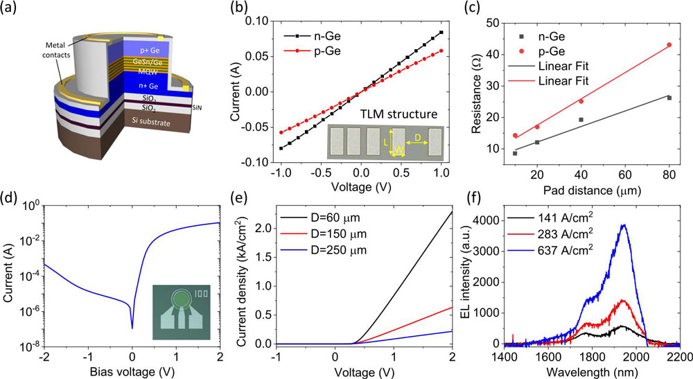
Figure 2. (a) 3D schematic of GeSn/Ge MQW VCSE photodiode. (b) Current−voltage curves of transmission line method structures on n-Ge and p-Ge with pad distance of 20μm. Inset: optical microscope image. (c) Extracted total resistance for n- and p-contacts with different pad distance. (d) Electrical characterization of GeSn/Ge MQW VCSE photodiode with mesa diameter of 250μm. Inset: typical fabricated MQW VCSE diode. (e) Current density−voltage curves of diodes with different mesa diameters. (f) Electroluminescence spectra of 60μm-diameter diode with different injection current densities.
VCSE p-i-n diodes were fabricated with a double-mesa structure, using CMOS compatible processing techniques (Figure 2). The structures were passivated with 400nm PECVD SiO2. The metal contacts consisted of titanium/titanium nitride/aluminium (Ti/TiN/Al). The contacts were rapidly thermally annealed to improve the ohmic contact between the n-Ge and the metal electrodes.
Under forward bias, smaller-diameter devices were found to respond with higher current density, suggesting more uniform current spreading. The emission spectrum wavelength of the devices apparently cuts off just above 2000nm (2μm), due to the reduced sensitivity in this range of the liquid-nitrogen-cooled indium gallium arsenide photodetector array.
Electrically pumped lasing was not observed at 637A/cm2, which exceeds the calculated radiative current density needed for positive optical gain. The team comments: “This suggests that non-radiative recombination and cavity losses within the device may be contributing to a higher injection current density requirement for lasing. To realize electrically pumped lasing from the VCSE diodes, future research can focus on several potential solutions, including improving material quality to suppress the non-radiative recombination, optimizing the cavity to reduce the cavity loss, or tuning the Sn(Si) concentration or strain in GeSn/Ge quantum wells to enhance gain.”
The author Mike Cooke is a freelance technology journalist who has worked in the semiconductor and advanced technology sectors since 1997.


