


News: Microelectronics
6 July 2023
Gallium oxide flash memory
King Abdullah University of Science and Technology (KAUST) in Saudi Arabia and the Indian Institute of Technology have claimed the first demonstration of an ultrawide-bandgap β-Ga2O3 flash memory [Vishal Khandelwal et al, Jpn. J. Appl. Phys., v62, p060902, 2023].
Ultrawide-bandgap materials like Ga2O3 are being projected for use in a wide and varying range of transparent, flexible, high-power, RF and extreme-environment electronics, along with ultraviolet (UV) photonics.
The flash memory device (Figure 1) was fabricated on a 50nm n-Ga2O3 layer on sapphire grown by pulsed laser deposition (PLD) from a silicon-doped Ga2O3 target. The growth temperature was 700°C, and the oxygen partial pressure was 4mTorr. The resulting film carrier concentration and mobility were 5x10¹⁸/cm2 and 0.35cm2/V-s, respectively, according to Hall measurements.
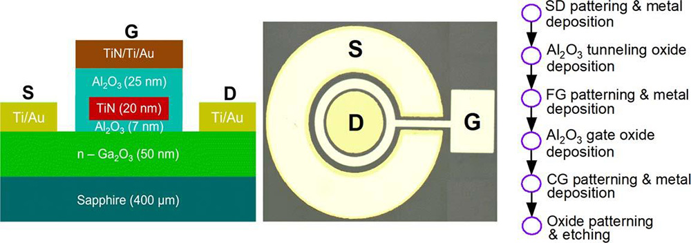
Figure 1: Flash memory device: (a) cross-sectional schematic; (b) top microscopic view; (c) fabrication process flow.
The fabrication sequence began with source/drain (S/D) formation using direct current (DC) and radio frequency sputtering of titanium (Ti) and gold (Au). The drain contact was 200μm diameter.
The aluminium oxide (Al2O3) tunneling (bottom) and blocking (top) layers were formed using atomic layer deposition (ALD). The titanium nitride (TiN) floating gate metal was applied using conventional photolithography/lift-off techniques. The inner and outer diameters were 240μm and 260μm, respectively.
The TiN/Ti/Au control gate was created using sputtering and photolithography. The inner and outer diameters were 220μm and 280μm, respectively. The effective gate length was around 30μm. The device was completed by etching away excess Al2O3 to expose the S/D contacts.
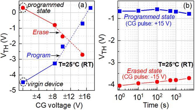
Figure 2: Flash memory characteristics at room temperature, 25°C: (a) VTH after program and erase operations; (b) retention characteristics.
The memory operation of the device used voltage pulses to charge and discharge the floating gate, enabling shifts in the threshold voltage (VTH) from negative, normally-ON, to positive, normally-OFF (Figure 2). The memory state could then be determined by the resistance between the source and drain.
Negative charge from injected electrons on the floating gate depletes the underlying n-Ga2O3 channel, increasing the resistance and VTH.
Given that p-type conductivity is not presently achievable on the Ga2O3 platform, the researchers believe the erase process is derived solely from ejecting electrons from the floating gate rather than hole injection, as implemented on silicon-based flash memory. The team suggests that post-deposition annealing (PDA) steps could improve the tunnel oxide layer for memory operations by minimizing trap density at the Al2O3/Ga2O3 interface.
The injected electrons are pulled onto the floating gate by a positive pulse on the control gate. A +17V 100ms pulse gave a VTH of +0.3V from a virgin value of −4.5V. Subsequent erase steps with negative pulses ejecting electrons from the floating gate did not restore the virgin threshold, but a memory window of more than 3V was obtainable, using ±15V pulses. The states were retained on the scale of 5000s (1.4 hours).
The researchers suggest that suitably programmed devices could be used as standalone normally-OFF low-voltage transistors. Further, given the difficulty in achieving p-type conductivity, CMOS-like power-efficient logic circuitry could come from combining normally-ON and programmed normally-OFF transistors.
The team explains: “Thus, the logic circuitry for controlling the β-Ga2O3 power converters can be realized using a suitable connection of virgin/erased (normally-ON) β-Ga2O3 flash memory device with a programmed (normally-OFF) β-Ga2O3 flash memory device. Consequently, the power converters and their logic control circuitry can be monolithically integrated into a standalone β-Ga2O3 substrate.”
The author Mike Cooke is a freelance technology journalist who has worked in the semiconductor and advanced technology sectors since 1997.


