


News: Suppliers
14 July 2023
DISCO unveils KABRA process optimized for GaN wafer production
Tokyo-based DISCO Corp – which makes semiconductor manufacturing equipment including chemical mechanical polishing (CMP) systems and laser-based ingot slicing equipment and processes – says that, using its KABRA (Key Amorphous-Black Repetitive Absorption) laser-based ingot slicing method, it has developed a process optimized for the production of gallium nitride (GaN) wafers that can simultaneously increase the number of GaN wafers produced and decrease the production time.
GaN requires time for crystal growth, and is a very delicate material as the ingots produced are small in diameter and thin. Conventionally, the mainstream method for slicing GaN ingots into wafers was to use a diamond wire saw. However, there were several problems when slicing with a wire saw, such as the processing time, material loss at the sliced sections that is thicker than the thickness of the wire used, and the low number of wafers produced due to material loss from the lapping process which is done after slicing to planarize the surface. These led to the wafers being expensive, and has hindered the spread of GaN power devices, reckons DISCO.
DISCO says that, since the KABRA process was developed for the production of silicon carbide (SiC) wafers, it has been receiving requests from many manufacturers to apply this process to GaN as well. DISCO has hence been putting effort into R&D to realize a KABRA process optimized for GaN, and is now announcing its readiness for mass production.
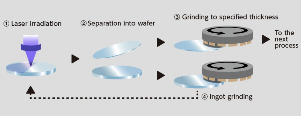
KABRA process flow for GaN wafer mass production
- The laser irradiates inside the ingot and a KABRA layer is formed;
- The ingot is separated into a wafer;
- The wafer is ground to the specified thickness;
- The ingot’s upper surface is ground for the next laser irradiation.
Properties of the new process are listed as:
Low material loss
- By controlling the position of the laser’s focal point in real time, slicing without thickness variation is possible;
- Unlike the wire saw, lapping is unnecessary, as there are no undulations after slicing.
High throughput
- Development of a special optical system and processing method optimized for GaN;
- Efficient creation of the KABRA layer (the processing mark and cleaved area are created by focusing the laser within the material) due to a short stage scanning distance.
High yield
- Efficient discharge of the nitrogen produced within the material and prevention of wafer breakage by also creating a uniform KABRA layer near the edge of the ingot.
Disco develops DAL7440 KABRA laser saw for 8-inch SiC wafers
Disco’s KABRA!zen fully automates KABRA laser slicing technology


