News: Suppliers
27 July 2023
Spalling-induced GaN lift-off and transfer
Air Force Research Laboratory, KBR Inc and Agnitron Technology in the USA have applied spalling-induced van der Waals (vdW) epitaxial lift-off (ELO) and transfer methods to 4-inch gallium nitride (GaN) films [Michael Snure et al, Journal of Applied Physics, v134, p025307, 2023].
VdW materials — such as graphite/graphene, molybdenum disulfide, and sp2-bonded boron nitride (BN) — have strong chemical bonds in two dimensions, but weaker van der Waals bonds in the third dimension. The researchers grew GaN on sapphire, using BN as an intermediate lift-off layer. The weak vdW bonds act like a sort of Velcro, enabling GaN to be separated without cracking from its growth substrate with suitable encouragement from a nickel (Ni) spalling layer.
The researchers describe their aims in their 2D material-based layer transfer (2DLT) work: “In developing a process to integrate GaN on sapphire epitaxial films, achieving a high-yield, rapid and controlled lift-off and transfer is necessary.” The hope is to improve performance, reduce costs, and develop new electronics structures for higher-power and more efficient radio frequency (RF) and light-emitting devices.
The choice of boron nitride as the vdW layer was motivated by its higher stability and material compatibility with GaN growth, compared with other potential vdW materials. BN is also the only one that is a dielectric, rather than being electrically conducting in some way. The team comments: “For the 2DLT process to become a viable commercial option, it will need to be scalable, fast and high yield. So far, growth and transfer of GaN have been mostly limited to smaller areas with a few reports on epitaxial growth and transfer at the 2-inch wafer scale using BN.”
The researchers grew BN films on 4-inch c-plane sapphire substrate, using metal-organic chemical vapor deposition (MOCVD). The precursors were triethylboron (TEB) and ammonia (NH3) in hydrogen carrier gas. The substrate was not subjected to surface preparation before loading into the MOCVD system. The sapphire surface was prepared in the reaction chamber by nitridation at 900°C, creating a thin aluminium oxynitride (AlON) layer to promote nucleation of BN.
The BN layer itself was grown for 15 minutes at 1200°C. The growth pressure was 20Torr, and the V/III ratio 3500. The result was 5-6 layers of BN, or around 2nm thickness. Since the BN was both the release layer and template for further III-N growth, it was critical that the layer was uniform and smooth. According to the x-ray reflectance measurements at 5mm intervals, the BN thickness was 2.03±0.03nm. The root-mean-square surface roughness was of order 0.25nm, according to atomic force microscopy (AFM).
Further MOCVD growth involved layers of AlN and GaN with trimethyl- precursors being used for the metal supply. Ammonia continued as the nitrogen source. AlN layers were grown at 1090°C, 60Torr and 2200 V/III ratio. The GaN was grown in three-steps on a 20nm AlN nucleation layer: 3D growth at 1090°C, high-temperature recovery at 1195°C, and fast growth at 1090°C. The first two steps were designed to reduce dislocations by producing 3D islands, which were then laterally coalesced to produce a uniform 1.9μm film.
The AlN nucleation layer thickness was optimized for good GaN quality with low residual strain. Thin AlN layers risk creating voids in coverage of the underlying BN, impacting GaN growth quality. Thicker layers suffer from surface roughness while also increasing the strain in the overlying GaN, factors that reduce crystal quality. The x-ray rocking curves indicated crystal quality comparable to other reports of GaN growth on vdW materials: 0.14 and 0.286° full-width at half-maximum (FWHM) for the (002) and (102) crystal planes, respectively.
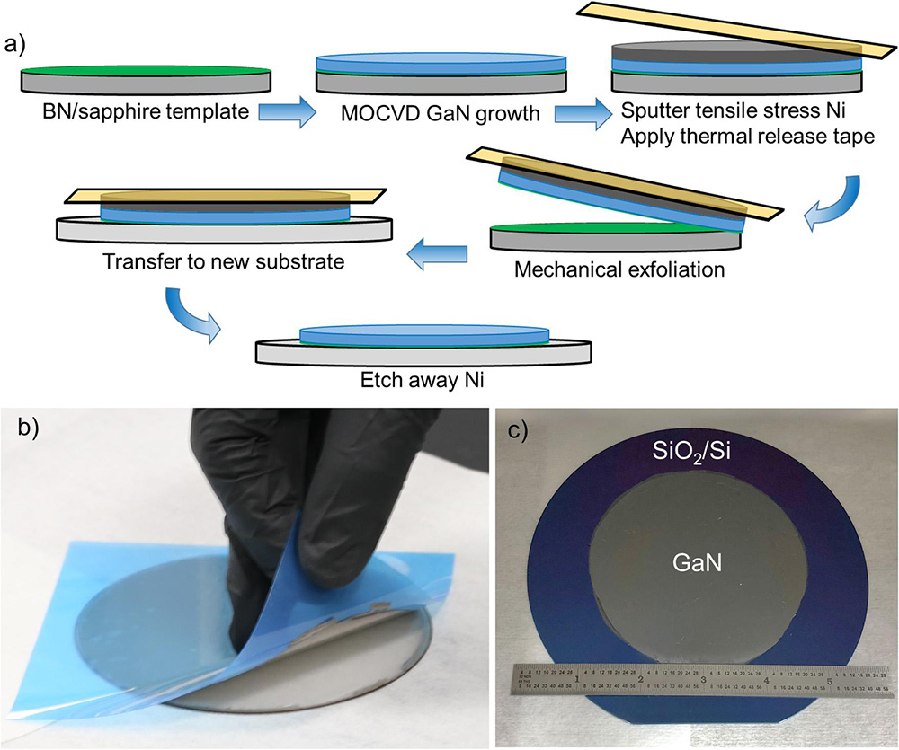
The wafer was prepared for the spalling-induced vdW lift-off and transfer process (Figure 1) by cleaning the GaN surface with solvent and oxygen plasma ashing. Nickel (Ni) was applied by radio frequency (RF) magnetron sputtering at 300W and 5mTorr pressure of the argon working gas. The nickel layer introduced tensile stress, enabling spalling removal of the GaN layer from the substrate. According to tests on silicon, a 4μm introduced 400MPa stress on average. The thickness of the Ni film had to supply enough energy to break the vdW bonds, releasing the GaN for lift-off, but not too much, to avoid cracking. The best results came from a 2μm Ni layer.

Figure 1: (a) Schematic process flow for transfer process. Images of (b) mechanical exfoliation step and (c) full 4-inch GaN film transferred to SiO2/Si wafer.
Thermal release tape (TRT) was used as a handle for the spalling release by exfoliation. The exfoliation process was initiated by scribing the edge of the GaN film. The lift-off process took less than 15 seconds. The TRT/Ni/GaN stack was then transferred to a 6-inch silicon dioxide/silicon (SiO2/Si) substrate, using double-sided tape.
Once the stack was in place, the TRT was removed, and the nickel stripped by Transene Company Inc’s Ni etchant TFB. The transferred films showed only a slight increase in x-ray rocking curve FWHMs. The team reports: “The most significant broadening is in the upper left region and near the edges, which is correlated with a visible crack in the upper left region caused by the transfer process.”
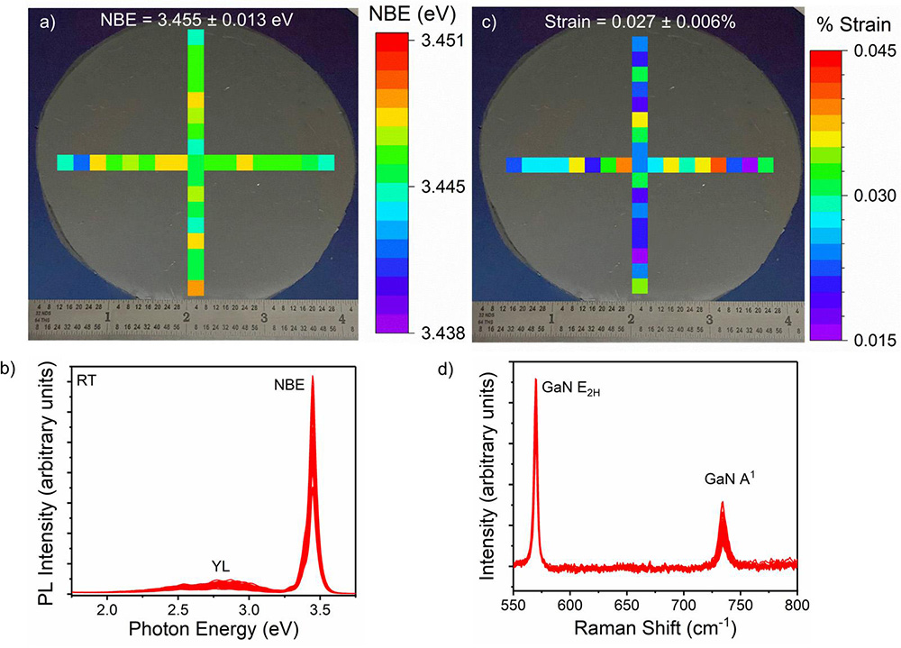
The researchers studied the optical properties of the transferred GaN layer transferred on the SiO2/Si wafer. The NBE PL peak position showed slightly higher variation, compared with the grown layer on BN/sapphire, while having about the same average value.
The most striking difference was in the strain values derived from Raman peak shift measurements. The GaN grown on BN/sapphire had about 0.25% compressive strain. During transfer, the presence of the 2μm Ni film was found to give 0.151% tensile strain to the GaN. The final layer after transfer was almost completely relaxed. It has been found by the team previously that Ni layers greater than 5μm leave tensile stress in the transferred GaN.

Figure 2: (a) Near-band-edge (NBE) photoluminescence (PL) peak position and (b) % strain measured by Raman spectroscopy. Plots of all GaN (c) PL and (d) Raman spectra.
The researchers comment: “This stepwise relaxation can be beneficial, reducing the formation of cracks that occur during the strain release.”
The author Mike Cooke is a freelance technology journalist who has worked in the semiconductor and advanced technology sectors since 1997.


