


News: Optoelectronics
5 January 2023
Room-temperature continuous-wave UV-C laser diode
Asahi Kasei Corporation and Nagoya University in Japan report on continuous wave (CW) lasing at room temperature in a 274nm-wavelength aluminium gallium nitride (AlGaN) [Ziyi Zhang et al, Appl. Phys. Lett., v121, p222103, 2022]. The lasing wavelength is in the ultraviolet C (UV-C) 100–280nm wavelength range, with photon energies of 12.4–4.43eV. The 274nm wavelength corresponds to 4.53eV.
The researchers report: “Although UV-C laser diodes have been demonstrated in prior work, CW lasing was not possible without cooling.” Hoped-for deployments of such devices include instrumentation, laser machining, and disinfection. Such applications require substantially increased efficiency and lifetime before commercialization would be possible.
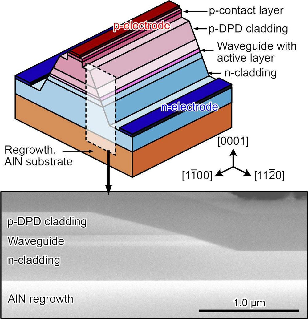
Figure 1: Schematic fabricated UV-C laser diode structure and cross-sectional scanning electron microscope (SEM) image of sloped mesa edge.
The material for the laser diode (Figure 1) was grown pseudomorphically on a 2-inch (0001) Al-polar AlN substrate (Figure 2), using metal-organic chemical vapor deposition (MOCVD). The waveguide layer included two 4.5nm quantum wells as an active photon-emitting layer. While the n-type used a traditonal silicon-doping strategy to tip the equilibrium to conduction by electron carriers, the bulk of the p-type doping was achieved through distributed polarization doping (DPD), which uses the varying charge polarization of AlGaN with different Al-contents to create hole conduction. Only the GaN cap layer was doped with magnesium (Mg) impurities to achieve p-type conduction. The use of DPD avoids the decreasing effectiveness of Mg as a p-type dopant in high- Al-content AlGaN. X-ray analysis confirmed the pseudomorphic nature of the AlGaN, showing the layers to be fully strained to match the AlN substrate lattice.
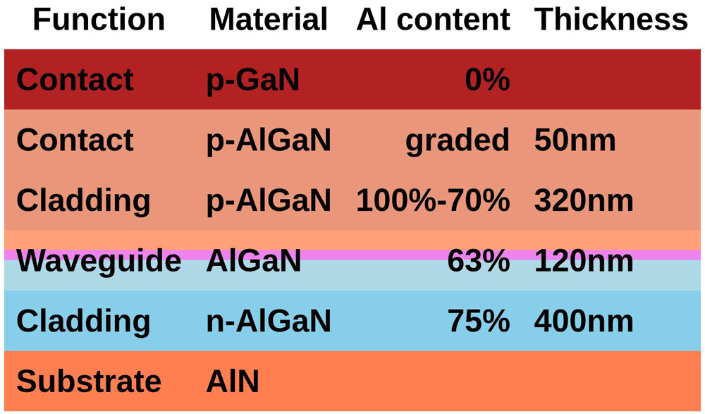
Figure 2: Material details.
The material was fabricated into 600μm-long devices. The sides of the laser diode mesa was bevelled at a 15° angle with the width of the top p-electrode of 5μm. The researchers explain the purpose of the bevel: “This angle was sufficiently shallow to effectively suppress dislocation formation that can result from the concentrated shear stress generated at the mesa edge.” This allowed the p- and 2xn-electrodes to be placed nearer to the mesa edge than previously, shortening the current flow path through the n-cladding and thus reducing series resistance. The cleaved end facets were coated to provide more than 90% reflectivity.
Pulsed operation (100ns at 0.02% duty cycle) was used to test the characteristics without thermal degradation. The peak wavelength at room temperature was 274nm and the thermal shift between -5°C and 65°C was 32pm/K, under current injection 10% above threshold. The characteristic temperature for the shift in threshold current (T0) was 70K. The horizontal and vertical far-field pattern (FFP) spreads were 6° and 30°, respectively, at 1mW output power. The horizontal pattern showed multiple peaks, presumably from different transverse modes. The multiple transverse modes also result in kinks in the emission power-current behavior, probably due to the stimulated emission hopping between these transverse modes.
The team comments: “It is expected that the linearity of L–I characteristics above the threshold current will be improved by reducing the number of allowed transverse modes, for instance, by using a narrower ridge and gain geometry or by eliminating higher-order modes by employing absorbing layers.”
One effect of using DPD p-doping, it is thought, was the series resistance being almost constant over the temperature range, unlike devices with Mg-doped cladding. The activation energy of Mg-doping is very high, resulting in large changes (reductions) in resistance of the cladding as the temperature increases.
The performance under continuous wave/direct current (CW/DC) operation with no thermal control at room temperature was compared with the pulsed results (Figure 3). The threshold current is 125mA, corresponding to 4.2kA/cm2 density. The CW voltage at threshold was 8.7V.
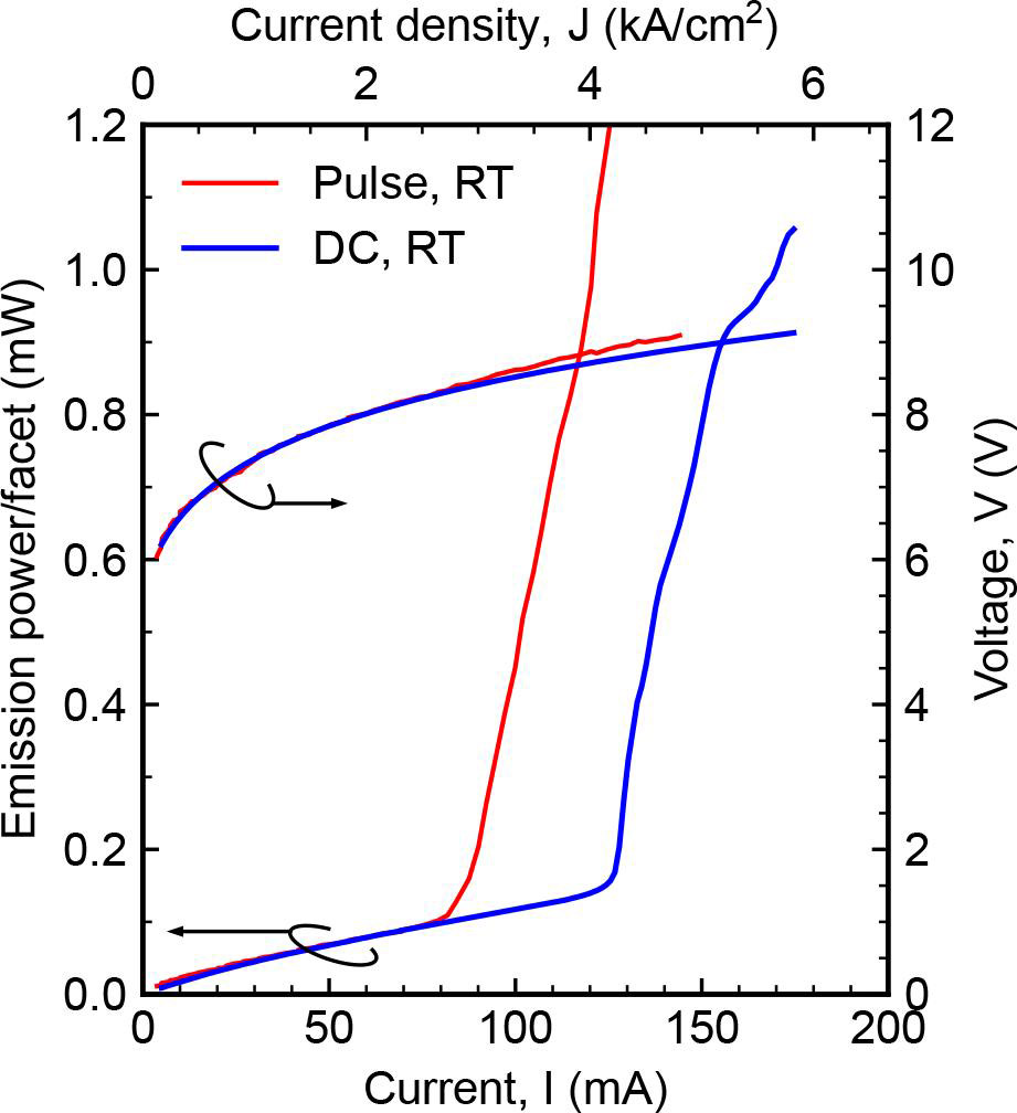
Figure 3: Emission power–current–voltage (L–I–V) characteristics of UV-C laser diode under pulsed and DC operation at room temperature.
The input power at threshold is estimated to increase the junction temperature by 28K above ambient through self-heating, consistent with the increased threshold current. This suggests that CW lasing requires reduced thermal resistance to heat dissipation and reduced heat generation from the series resistance, along with higher T0. The reduction in series resistance to 8.4Ω, from 12Ω in the team’s previous work, was key to achieving CW lasing at room temperature.
The team also thinks that better understanding of the factors impacting T0 could increase it towards the 150K level of commercial indium gallium nitride laser diodes. Such factors could include “broadening of the gain spectrum (decreasing the gain), thermally activated carrier escape, free-carrier absorption, and Auger recombination”.
The author Mike Cooke is a freelance technology journalist who has worked in the semiconductor and advanced technology sectors since 1997.


