


News: Microelectronics
9 February 2023
InGaAs QW HEMT for 6G communications
Researchers based in South Korea and Japan have reported optimized indium gallium arsenide (InGaAs) quantum well (QW)-channel high-electron-mobility transistors (HEMTs) with what is claimed to be record balanced frequency performance (Figure 1) [Wan-Soo Park et al, IEEE Transactions on Electron Devices, published online 10 January 2023.].
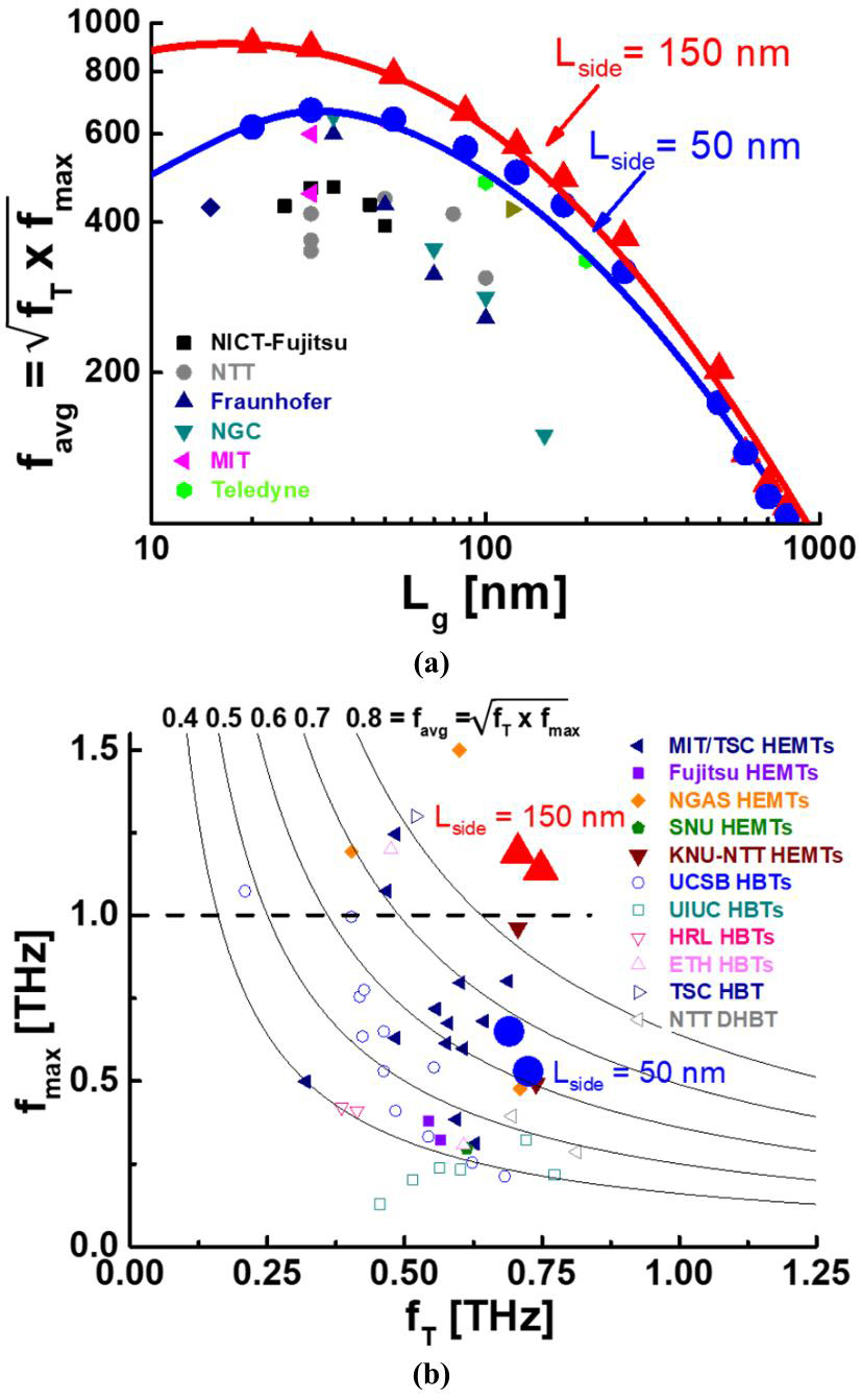
Figure 1: (a) Benchmark of favg versus gate length (Lg) for devices with different side-recess spacing (Lside) and those for other group reports on III–V HEMTs. (b) Benchmark of fmax as a function of fT for various devices compared with the team’s.
The team from Kyungpook National University and Quantum Semiconductor International Inc (QSI) in South Korea and NTT Corp in Japan, comment: “To the best of our knowledge, the In0.8Ga0.2As QW HEMTs with Lside = 150nm in this work exhibit the highest favg at all gate lengths in any III–V HEMT technology and the best balance of fT and fmax in any transistor on any material system.”
The various cut-off frequencies refer to different gain parameters. The T cut-off refers to current gain, while fmax refers to Mason’s unilateral (power) gain (Ug). The researchers explain: “fmax is a more appropriate figure of merit for analog and mixed-signal applications for which the transistor provides a power gain.” The favg value consists of the geometric mean of these two cut-off frequencies.
The team sees its achievements as contributing to meeting the demands of ‘Edholm’s law’, a Moore’s Law-like prescription for convergence of wired, wireless and nomadic capabilities as frequencies enter the sub-millimeter wavelength range for sixth-generation (6G) communications.
A key component of the work was optimizing Lside “as an effective remedy to mitigate the peak electric field intensity at the drain side of the gate, helping to reduce the intrinsic output conductance (goi) in aggressively scaled-down devices.”
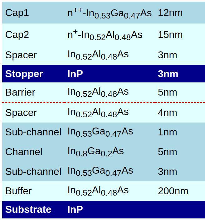
Figure 2: Material for HEMTs. Red dashed line represents silicon δ-doped layer.
The material (Figure 2) for the QW HEMTs was grown on semi-insulating (100) indium phosphide (InP) substrates, using metal-organic chemical vapor deposition (MOCVD).
In the fabricated HEMTs (Figure 3), a gate-recess was implemented with InP used as an etch-stop layer. The recessing gave a gate–channel distance (tins) of about 5nm.
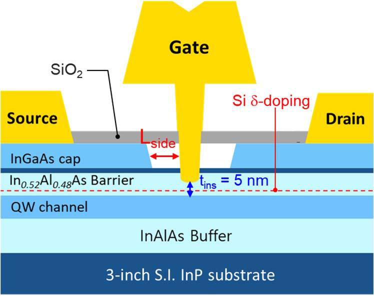
Figure 3: Schematic sketch of In0.8Ga0.2As QW HEMT.
The doped cap had a two-layer structure to enhance tunneling efficiency between the QW channel and the source/drain contacts.
Without the capping layer the structure exhibited a two-dimensional electron gas (2DEG) of 1.78x10¹²/cm2 density and 13,500cm2/V-s mobility, according to Hall measurements.
The source–drain distance was 1μm. The ohmic source/drain electrodes consisted of titanium/molybdenum/titanium/platinum/gold (Ti/Mo/Ti/Pt/Au). The devices were isolated using mesa etching. The source/drain space was insulated with plasma-enhanced chemical vapor deposition (PECVD) silicon dioxide (SiO2). The T-gate was formed in the source–drain space, consisting of Pt/Ti/Pt/Au.
The researchers took particular care to control the side-recess spacing (Lside) by controlling the gate recess etch time. The gate length (Lg) varied between 300nm and 20nm. Some HEMTs were fabricated with longer gates between 10μm and 0.5μm, using an i-line 365nm ultraviolet stepper rather than electron-beam lithography.
Devices with 20nm Lg and 150nm Lside demonstrated a cut-off frequency (fT) of 0.75THz, extrapolated from 1–50GHz measurements. The 1.1THz maximum oscillation frequency (fmax) was derived from a small-signal model rather than measured directly from Ug, which was “challenging” to extrapolate. Reducing Lside to 50nm gave a similar fT of 0.72THz, but there was a significant impact on fmax, which declined to 0.53THz.
The enhancement of the wider Lside on fT was attributed to reduced delay times as a result of improvements in short-channel effects (SCEs). The researchers add: “Most importantly, the device with a wider Lside led to a far better fmax behavior due to the suppressed intrinsic output conductance (goi).”
Among the SCEs improved by the wider 150nm Lside was a drain-induced barrier lowering (DIBL) value to 60mV/V, compared with 110mV/V for 50nm.
The team sees reducing the equivalent oxide thickness (EOT) between the gate and channel as key to accessing further improvements in frequency performance. However, the Schottky gate setup limits the ability to simply reduced the barrier thickness, which would at the same time increase gate leakage. The researchers comment: “In this regard, the use of an MIS [metal-insulator-semiconductor] scheme with high-k dielectric layers would help to not only scale down EOT but also effectively suppress the gate leakage current.”
InGaAs QW HEMT InGaAs HEMT InP substrates MOCVD
The author Mike Cooke is a freelance technology journalist who has worked in the semiconductor and advanced technology sectors since 1997.


