


News: Microelectronics
28 December 2023
Dynamic performance of vertical GaN JFETs
Virginia Polytechnic Institute and State University and NexGen Power Systems Inc in the USA have claimed the first experimental characterization of dynamic on-resistance ( RON) and threshold voltage (VTH) stability in vertical gallium nitride (GaN) power transistors [Xin Yang et al, IEEE Transactions On Electron Devices, published online 5 December 2023]. The researchers studied NexGen junction field-effect transistor (JFET) devices rated at up to 1200V (1.2kV).
Dynamic RON describes the increased resistance of switched transistors relative to the value in a steady DC state. The team comments: “This issue can induce a higher conduction loss of the device and a degraded device lifetime in applications.”
The researchers compared the performance of NexGen’s 650V/200mΩ- and 1200V/70mΩ-rated GaN JFETs (Figure 1) against that of commercial 650V and 1200V silicon carbide (SiC) metal-oxide-semiconductor FETs (MOSFETs, IMZA65R083M1H, C3M0075120D), and 650V GaN high-electron-mobility transistor with Schottky-type p-GaN gate (SP-HEMT, GS-065-011-1-L).
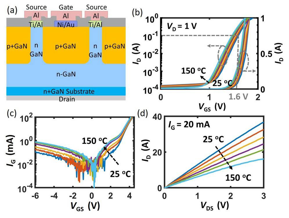
Figure 1: (a) Schematic of vertical GaN JFET. Characteristics at 25-150°C with 25°C incremental step of 1.2kV device: (b) transfer, drain current (ID) versus gate potential (VGS) on log and linear scales; (c) IG versus VGS; and (d) output.
NexGen’s devices were fabricated on 100mm bulk n+-GaN substrates. The fin channels were around 1μm high and sub-micron in width. The gate consisted of implanted p-GaN regions between the fins. The drift region between the fin channels and the drain was around 8μm and 10μm for the 650V and 1200V devices, respectively. The corresponding avalanche breakdown voltages were estimated to be 800V and 1500V.
The threshold voltage (VTH) of the 1.2kV JFET was 1.6V at 25°C, decreasing to 1.45V at 150°C. The RON at 20mA IG was around 70mΩ at 25°C, increasing to 150mΩ at 150°C.
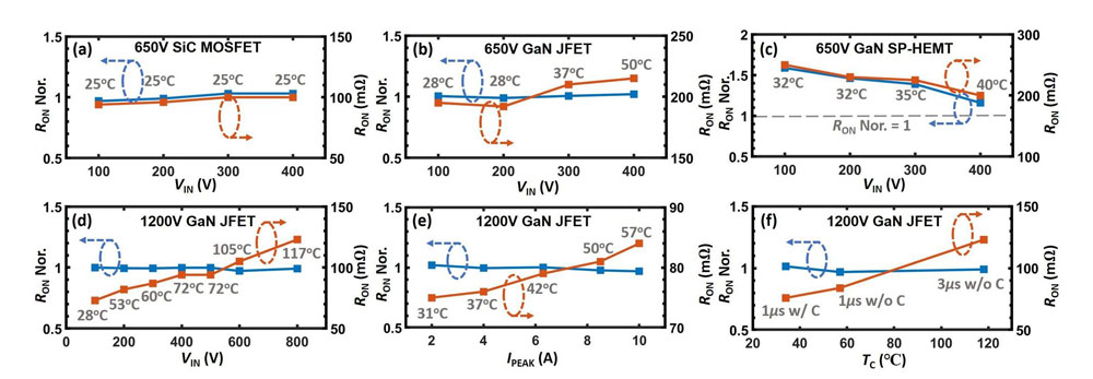
Figure 2: Extracted dynamic RON and normalized dynamic RON versus VIN with 3μs pulse width for 650V-rated (a) SiC MOSFET, (b) GaN JFET, (c) GaN SP-HEMT, and (d) 1200V GaN JFET. (e) and (f) Dynamic RON performance of 1200V GaN JFET at 800V VIN (10A steady state) versus 1μs pulse peak drain current and TC with/without cooling, respectively.
The researchers used continuous, hard-switching double pulse tests (DPTs) with an active measurement circuit to assess the dynamic RON performance (Figure 2). The devices were assembled in dual flat no-lead (DFN) packages, and case temperature (TC) was determined using thermal imaging. Fan cooling was applied to the SiC MOSFET and GaN SP-HEMT comparison devices, but not to the GaN JFETs. The RON values were normalized according to the static RON at the measured TC.
The researchers comment: “The results show 650V and 1200V GaN JFETs are both dynamic RON free.”
The researchers also performed static stress testing to determine how stable the RON and VTH values were, as relevant to application scenarios where the power device is mostly off. The maximum VTH and RON shifts for the 1200V JFET were 0.05% and 1.38%, respectively. By contrast, a 650V GaN SP-HEMT has corresponding shifts of order 20% and 10%.
The researchers also compared simulations of JFET and HEMT structures to analyze the difference in dynamic RON and static stability performance. The team suggests that a key difference arises in the position of the peak electric field, which usually arises near the edge termination. In the HEMT structure, the peak field is only 20-30nm from the device surface, while in the JFET peak E is buried about a 1μm away from the surface. Combined with the lower defect density in epitaxial layers grown on bulk GaN, surface and buffer traps are largely suppressed, reducing delays in state changes, which almost eliminates the dynamic RON in the GaN JFET, it is thought.
The researchers add: “Finally, the native p-n junction gate in JFET has no band discontinuities, enabling the more efficient carrier supply or extraction as compared to the p-GaN/AlGaN/GaN hetero-gate in the HEMTs (particularly with the Schottky contact to p- GaN in SP-HEMT).”
The author Mike Cooke is a freelance technology journalist who has worked in the semiconductor and advanced technology sectors since 1997.


