


News: LEDs
8 December 2023
V-defects for improved red InGaN LED performance
University of California Santa Barbara in the USA has been exploring the potential for V-defects to improve the performance red/orange light-emitting diode (LED) devices with high-indium-content indium gallium nitride (InGaN) multiple quantum wells (MQWs) [Jacob J. Ewing et al, Optics Express, v31, p41351, 2023].
The team reports 6.5% peak external quantum efficiency (EQE) for a device on patterned sapphire substrate (PSS), “which is one of the highest reported efficiencies in the academic literature for red/orange InGaN LEDs on PSS,” adding: “This result is important because PSS is widely used in the LED industry and represents a cost-effective, high-light-extraction substrate for mass production of InGaN LEDs.”
Although much effort has been expended on reducing defect formation in the the InGaN system, for long-wavelengths V-defects that nucleate on threading dislocations have been found to improve hole injection efficiency through {10-11} semi-polar sidewalls in an inverted pyramid formation.
V-defects nucleate more readily in III-nitride structures grown on silicon (Si). Indeed, Nanchang LED company has reported 27.5% wall-plug efficiency (WPE) at around 600nm wavelength and 16.8% WPE at 620nm at 0.8A/cm2 injection by using a GaN-on-Si template and V-defect engineering.
Implementing V-defect benefits on PSS is much more challenging. InGaN on PSS tends to have lower defect densities compared with materials grown on silicon or flat sapphire. On the other hand, PSS devices tend to have higher light extraction efficiency due to light scattering from the patterned sapphire surface, which reduces total internal reflection. With flat top and bottom surfaces, total internal reflection impedes light being emitted from InGaN LED structures.
The UCSB team used atmospheric-pressure metal-organic chemical vapor deposition on GaN on PSS and (111) silicon (Si) to grow the epitaxial structure (Figure 1) for the InGaN LEDs. The GaN on PSS template consisted of 2.75 μm Si-doped n-GaN. The GaN-on-Si was supplied by Enkris Semiconductor Inc (800nm buffer, 2 μm unintentionally doped, and 2 μm Si-doped).
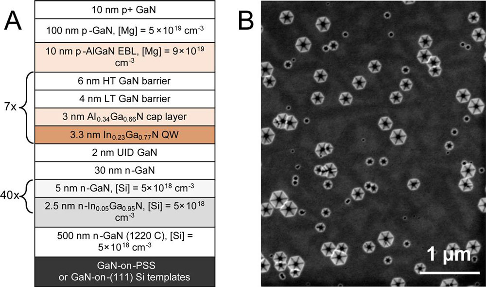
Figure 1: (a) Epitaxial structure for red InGaN LEDs; (b) SEM image of growth surface showing unfilled V-defects.
The UCSB structure included a 40-period superlattice designed to nucleate large V-defects and capture impurities before the 7-period MQW active region. The superlattice and MQW layers were grown at 920°C and 775°C, respectively, according to thermocouple readings. The barriers between the wells were grown in low- and high-temperature steps (LT and HT). An aluminium gallium nitride (AlGaN) cap on the wells suppressed indium desorption during the higher-temperature barrier growth. The structure was completed with magnesium-doped electron-blocking (EBL) and p-contact layers.
LEDs and μLEDs were fabricated with 110nm indium tin oxide (ITO) transparent p-contact, 700nm-high mesas, silicon dioxide/tantalum pentoxide/aluminium oxide (SiO2/Ta2O5/Al2O3) omnidirectional reflector (ODR), and atomic layer deposition (ALD) SiO2 sidewall passivation. The metal contacts were aluminium/nickel/gold.
Photoluminescence from the quantum wells fell mainly in the range 500-650nm. Some emissions around 420nm came from the sidewalls of the V-defects where the QWs are thinner and contain less indium. The epitaxial material on GaN/Si exhibited intensity oscillations from Fabry–Pérot interference between light reflected at the flat top and bottom surfaces. The material on PSS had a smoother PL spectrum since light scattering from the patterned surface interrupted the Fabry–Pérot effect.
The researchers report peak external quantum efficiency (EQE) and wall-plug efficiency (WPE) of 6.5% and 3.5%, respectively, for a packaged and fully encapsulated LED of area 0.1mm2. The EQE peaked at 28A/cm2 injection, and the WPE at 20A/cm2. Between 20A/cm2 and 28A/cm2 the wavelength blue-shifted from 595nm to 590nm. At lower injections the wavelength exceeded 600nm, while at 100A/cm2 the wavelength shortened to around 575nm.
The researchers comment: “The blue shift is a result of screening of the large electric field in the QWs by injected carriers. The high efficiency is attributed to lateral injection through the semi-polar sidewalls of V-defects as well as the enhanced light extraction from PSS. It’s also plausible that the V-defects could enhance light extraction by roughening the top surface. However, if the p-GaN growth conditions are optimized to fill the V-defects completely then this effect would be mostly eliminated.”
With a view to future improvement, the team performed a range of analyses of the epitaxial material on PSS. In TEM imaging the researchers found large V-defects (VD) and a number of other defects. The latter likely enable non-radiative recombination of electron and holes, reducing light output power and efficiencies in LED devices. In particular, the TEM imaging showed the presence of a stacking fault box (SFB), “very likely to be a significant non-radiative center,” according to the team. The researchers hope that improved growth techniques will lead to the elimination of SFB and reduced numbers of undesired defects.
Another concern was the relatively low density of V-defects: around 1x10⁸/cm2. The researchers comment: “This density is much lower than the density achieved on (111) Si by the Nanchang LED company and may be one of the reasons for increased voltage and lower WPE on the PSS LEDs.
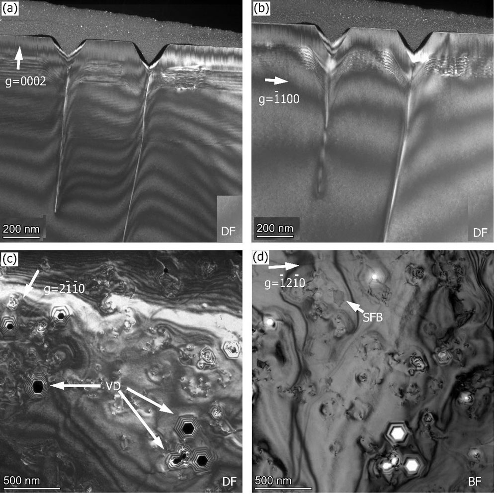
Figure 2: (a) Zone-axis and (b) non-zone-axis dark field (DF) scattering contrast transmission electron microscope (TEM) images of red LED on PSS. (c) Dark-field plan-view TEM image. (d) Bright-field (BF) plan-view TEM image.
To achieve complete lateral injection the spacing of V-defects needs to be lateral diffusion length which is ~100nm.” At the density seen in the TEM images, the average distance between V-defects is around 1 μm, about 10x the diffusion length. In particular, at this distance the holes find it difficult to distribute themselves uniformly through the wells, due to alloy fluctuation effects.
https://doi.org/10.1364/OE.503732
The author Mike Cooke is a freelance technology journalist who has worked in the semiconductor and advanced technology sectors since 1997.


