


News: Optoelectronics
14 December 2023
Laser-assisted separation for freestanding GaN
Osaka University in Japan has reported on a laser-assisted separation (LAS) technique for freestanding gallium nitride (GaN) grown by the sodium-flux technique from a seed layer on sapphire [Kazuma Hamada et al, Jpn. J. Appl. Phys., v62, p125503, 2023].
Creating freestanding and bulk GaN is seen as important for producing a wider range of GaN optical and power capabilities, using the material’s wide bandgap, high breakdown field, and high thermal conductivity.
The LAS consisted of decomposing parts of the GaN seed by laser irradiation through the sapphire substrate before the main GaN crystal growth process. Sapphire is transparent to deep ultraviolet light, while GaN is highly absorbing.
The team comments: “Since this technique reduces the contact area between the sapphire and GaN, separation occurs spontaneously during the cooling process after growth. We found an appropriate LAS processing pattern for separation and successfully obtained freestanding GaN crystal without cracks.”
The researchers further applied the LAS technique to multi-point seed (MPS) crystal growth, enabling crystal GaN thicker than usual with MPS without LAS preparation.
The GaN/sapphire seed substrates were grown using metal-organic chemical vapor deposition (MOCVD). The interface between the GaN and sapphire was patterned by LAS decomposition of the GaN (Figure 1): a reference without LAS, and a simple and more complex patterning resulted in three test samples.
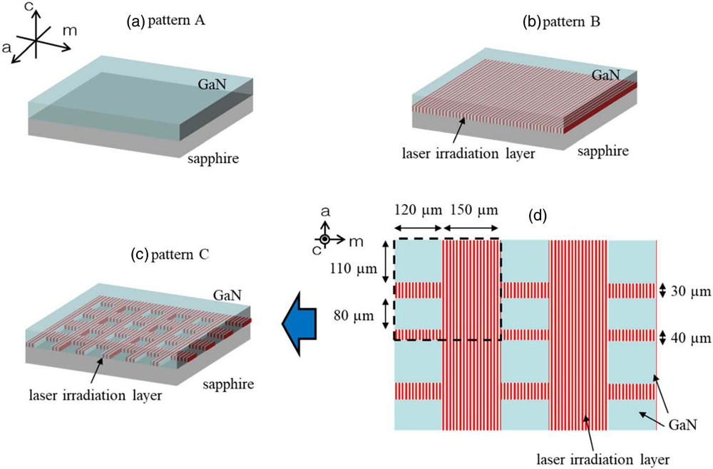
Figure 1: Schematic of seed crystals. (a) Pattern A: c-plane GaN/sapphire grown by MOCVD without LAS, (b) Pattern B: LAS over entire surface. (c) Pattern C: partial LAS. (d) Detail of pattern C.
The crystal growth consisted of placing the samples in a 19mm-diameter alumina crucible. The crucible was inserted into a glovebox with Ga, Na and carbon in an argon atmosphere. The box was evacuated and then nitrogen was introduced at 1MPa pressure. The temperature was increased to 870°C and the nitrogen pressure to 4MPa. The growth was carried out for 24 hours, resulting in a GaN layer about 500μm thick.
The unpatterned seed (sample A) resulted in cracked materials, both the GaN and sapphire. For the simple LAS patterned sample B, the GaN was uncracked, but the sapphire substrate did crack. The more complex partial LAS pattern of sample C resulted in both parts, sapphire and GaN, being uncracked. Further, only sample C gave separated freestanding GaN.
X-ray analysis of diffraction peak shifts was used to assess the radius of curvatures of the samples (Table). The sample C was much flatter, as indicated by the much larger radii of curvature.
Table: Radii of curvature of GaN crystal grown on seed crystal with pattern A, pattern B, and pattern C along the a-axis and m-axis.
Axis |
Pattern A | Pattern B | Pattern C |
| a- | 0.93m | 0.94m | 16.4m |
| m- | 1.23m | 0.86m | 9.25m |
The researchers comment: “In general, it is known that a GaN/sapphire substrate curves in a convex shape because sapphire has a larger thermal expansion coefficient than GaN. The presence of a convex shape in the grown crystal indicates that it is still under stress from the sapphire during the cooling process. In particular, the crystal grown on seed with pattern B had the same curvature as the crystal grown on unprocessed GaN/sapphire and also had cracks, suggesting that this pattern does not promote separation. In addition, we observed that it was easier to separate GaN with pattern C, where a part of the GaN was completely decomposed with the lattice pattern, compared to pattern B, where laser irradiation did not immediately separate GaN over the entire surface.”
Working on the theory that the curvature was affected by the effective contact area between GaN and sapphire, the researchers tried reducing the area by using a higher LAS laser intensity on samples with the simple pattern B. Unfortunately, the seed layer separated from the sapphire before a crystal growth process could be applied. Hence, the researchers favor an LAS process using sample pattern C, in which part of the GaN is completely decomposed in a lattice pattern.
Cathodoluminescence (electron-beam excitation) was used to assess the dislocation density in the grown GaN, giving a value around 106/cm2 for all the samples. This compares with the higher value for the GaN seed layer of 108/cm2, a value typical for MOCVD.
The team combined the LAS method with MPS, where the seed layer consisted of 250μm-diameter circular GaN point-seed regions in a hexagonal array, separated by 550μm. Without LAS, the MPS method resulted in cracked GaN and sapphire material when the growth reached 600μm (Figure 2). Using a LAS substrate with MPS regions, the cracking was eliminated.
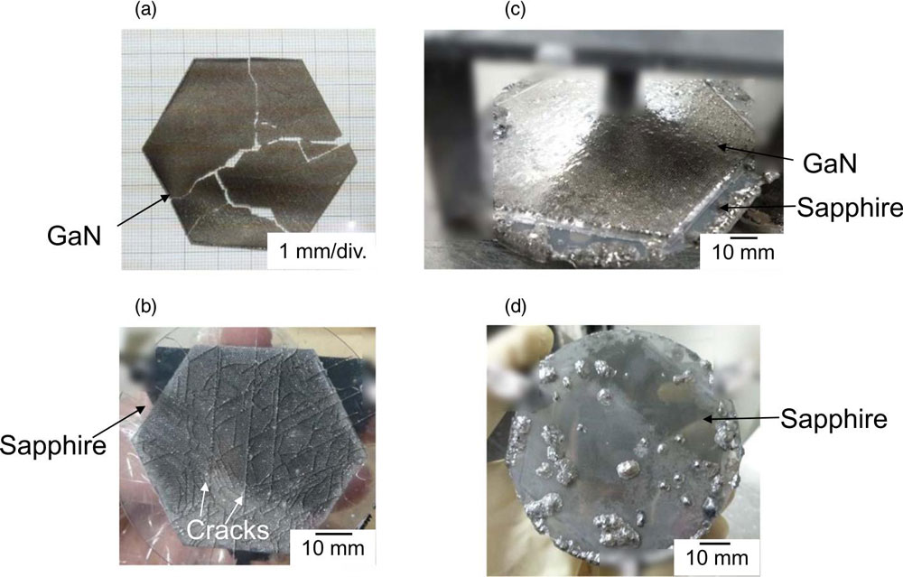
Figure 2: Optical images of grown crystal (a) on MPS substrate viewed from GaN surface and (b) viewed from sapphire surface; (c) grown crystal on LAS-MPS substrate viewed from GaN surface and (d) from sapphire surface.
The researchers comment: “The contact area between GaN and sapphire was reduced to the smallest achieved thus far, significantly reducing the tensile stress from the sapphire. The threading dislocation density was found to be comparable to that of conventional MPS substrates, indicating no deterioration.”
Laser-assisted separation GaN MOCVD Sapphire
https://doi.org/10.35848/1347-4065/ad0a45
The author Mike Cooke is a freelance technology journalist who has worked in the semiconductor and advanced technology sectors since 1997.


