News: Microelectronics
17 August 2023
Balancing charge to boost Ga2O3 breakdown beyond 10kV
Researchers based mostly in the USA report lateral gallium oxide (Ga2O3) Schottky barrier diodes (SBDs) with a charge-balancing nickel oxide (NiO) reduced surface field (RESURF) structure that boosted breakdown voltages (BVs) to more than 10kV [Yuan Qin et al, IEEE Electron Device Letters, v44, p1268, 2023]. The BV performance was thermally stable with more than 10kV blocking up to 200 °C.
The team from Virginia Polytechnic Institute and State University, University of Southern California, the US Naval Research Laboratory in the USA and Novel Crystal Technology Inc in Japan reports: “Our RESURF Ga2O3 SBDs show the highest BV, and the operational temperature is among the highest in multi-kilovolt Ga2O3 devices.”
The researchers see potential for their SBD design in medium- and high-voltage, high-temperature applications. The medium-voltage range above 1kV covers deployment in electric grid, motor drive, and renewable energy processing. The market is presently dominated by silicon bipolar technology, which suffers from slow switching speed.
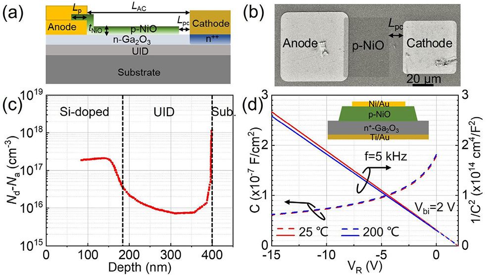
The SBDs (Figure 1) were fabricated on Ga2O3 substrates with an n-type Ga2O3 epitaxial layer. The anode region doping was boosted using silicon ion implantation, which was activated by 925 °C annealing in nitrogen. The cathode was titanium/gold (Ti/Au) annealed at 475 °C, and the anode nickel/gold (Ni/Au). Between the cathode and anode formations, the device region was isolated using nitrogen ion implantation.

Figure 1: (a) Schematic cross-section and (b) top-view scanning electron microscope (SEM) image of fabricated lateral Ga2O3 RESURF SBD. (c) Nd–Na depth profile of Ga2O3 epilayers (initial depletion width of Schottky contact ~85nm). (d) Capacitance–voltage (C–V) and 1/C2–V characteristics of vertical NiO/Ga2O3 diode at 25 °C and 200 °C.
The aim of the sputtered NiO RESURF structure was to balance depletion charges in the n-Ga2O3 channel at high voltage. Depletion at high forward bias shrinks the effective cross-sectional area for current flow, increasing on-resistance (Ron).
The p-type hole concentration of NiO has been found to be controlled via the oxygen partial pressure during sputtering. The researchers comment: “To reduce the impact of tNiO variation on charge balance and enable a larger process latitude, a lower Na is preferred.”
The team used a pure argon atmosphere, to reduce the hole concentration as much as possible, and the sputtering from a NiO source was carried out at room temperature. The p-NiO was annealed at 275 °C in nitrogen gas.
From capacitance–voltage measurements on a p-NiO/n-Ga2O3 vertical p–n heterojunction diode, the researchers estimate that the acceptor concentration (Na) from the NiO sputtering process was 8x10¹⁷/cm3 at 25 °C.
The thickness of the NiO device RESURF layer (tNiO) was designed to keep the charge imbalance margin below 15%. There was also a gap (Lpc) between the p-NiO RESURF layer and the cathode to avoid punch-through and leakage conduction. The NiO material was also extended onto the anode surface to a distance of 5 μm. The anode was then covered with a second Ni/Au application.
The device was then annealed at 275 °C to stabilize the acceptor concentration and to reduce NiO/Ga2O3 interface states. Passivation with photoresist completed the SBD processing.
A 75nm NiO RESURF layer enabled the team’s SBDs with anode–cathode distances (LAC) of 30 μm and 50 μm to exceed 10kV breakdown voltage, the measurement limit of the test equipment. The average electric field (Eave) in the drift region between the anode and cathode was thus more than 3.3MV/cm. For the 30 μm LAC SBD, a reference device without the NiO RESURF structure only achieved a BV of 2.8kV.
The leakage current at 10kV reverse bias was 2x10⁻⁶A/mm, ten times lower than reported for gallium nitride (GaN) SBDs.
A 17 μm LAC device had more than 8kV BV, corresponding to an Eave of 4.7MV/cm. The BV reduced to 6.1kV at 200 °C, giving 3.6MV/cm c.
The researchers comment: “The BV’s negative temperature coefficient (ηT) suggests the lack of avalanche breakdown and implies a trap-assisted breakdown mechanism.” The team points out that the achieved range of Eave exceeds the critical fields for GaN and silicon carbide (SiC). GaN lateral SBDs have been reported with ~1MV/cm Eave and 10kV BV.
The RESURF structure had a negative impact on (differential) Ron, increasing it by about a factor of 2, relative to Ga2O3 SBDs without RESURF.
The Baliga figure of merit (FOM, BV2)/Ron), which balances the effect of breakdown and forward current flow, is improved for the RESURF devices by a factor of more than 5, compared with reference SBDs without.
Electrical parameters, such as turn-on voltage (Von), Schottky barrier height, and ideality factor, were similar for all devices, coming in at around 1V, 0.74eV, and 1.2, respectively.
Increasing the operating temperature to 200 °C almost doubled Ron, while Von reduced to 0.7V. The on/off ratio was more than 106, even at 200 °C.

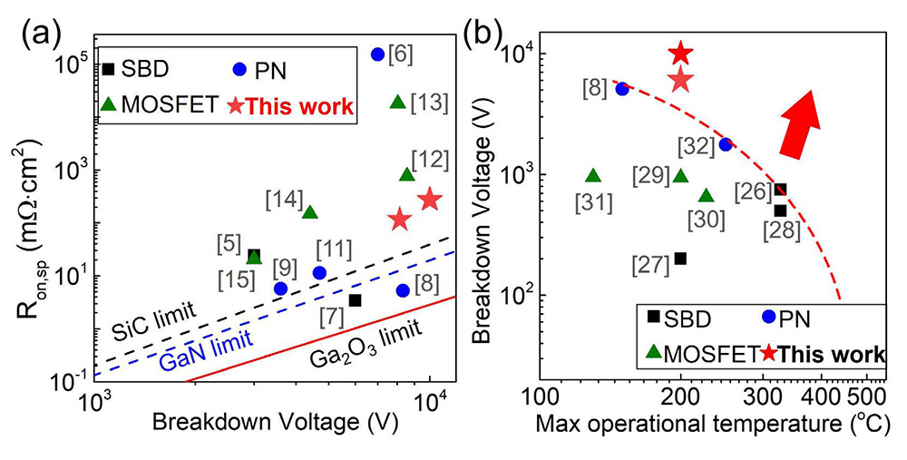
Figure 2: Benchmarks of team’s device (”This work”) against competition: (a) differential specific on-resistance (Ron,sp) versus BV for reported Ga2O3 SBDs, p–n diodes, and transistors with BV more than 3kV. (b) The BV versus maximum operational temperature for reported high-temperature Ga2O3 SBDs, p–n diodes, and transistors with BV more than 100V. Dotted line shows approximate boundary of prior data. Arrow shows desirable target. Note that 10kV BV of higher-BV device reflects measurement limit rather than actual BV.
The researchers present benchmarks of the BV and Ron,sp/maximum operation temperature (Figure 2). The researchers comment: “The Baliga’s FOM of 17 μm-LAC devices is 906MW/cm2 at 25 °C. The FOM of the 200 °C-operational, 10kV-class device (LAC = 30 μm) is at least 370MW/cm2 at 25 °C (the true FOM is expected to be much higher due to BV > 10kV).”
Gallium oxide Schottky barrier diodes
The author Mike Cooke is a freelance technology journalist who has worked in the semiconductor and advanced technology sectors since 1997.


