News: Optoelectronics
3 August 2023
MOCVD mid-to-long wavelength IR quantum cascade lasers on silicon
Researchers based in the USA report 8.1 μm-wavelength quantum cascade lasers (QCLs) grown on silicon (Si) by MOCVD [S. Xu et al, Appl. Phys. Lett., v123, p031110, 2023]. The team from University of Wisconsin Madison, University of Illinois Urbana-Champaign, and MicroLink Devices Inc, comments: “There are no prior reports of QCLs grown by metal-organic chemical vapor deposition (MOCVD) on silicon substrates.”
Such integration on silicon could lead the way to chip-scale, reliable and mass-producible photonic integrated circuits (PICs). The researchers contrast this with other integration methods such as wafer bonding: “Hybrid integration methods rely on accurate alignment for efficient waveguide-to-laser optical coupling, which, in turn, requires tight fabrication processing tolerances. Direct integration onto silicon by heteroepitaxy enables the potential for mid-infrared (IR) optoelectronics integrated with mature CMOS-compatible silicon platforms at low cost and with high throughput.”
Mid-infrared QCLs are typically grown on indium phosphide (InP). The team took particular care in creating a virtual InP substrate on silicon, using a combination of molecular beam epitaxy (MBE) and MOCVD. MOCVD is preferred over MBE in production. The researchers comment: “The technical challenge remaining is to overcome the defects and epitaxial growth-related issues, which arise from the large lattice-constant and thermal-expansion mismatch between native substrates, such as InP and silicon (e.g. ~8% lattice mismatch and ~50% thermal-expansion coefficient mismatch).”

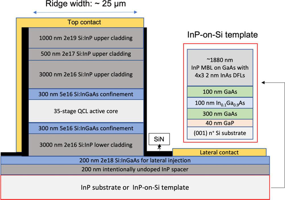
Figure 1: Full 35-stage, lattice-matched QCL structure, with 25 μm-wide ridge and lateral-current injection architecture, grown on InP substrate or on InP-on-Si composite template. Inset: structural details of InP-on-Si template with InAs dislocation filter layers (DFLs).
The arsenide part of the template structure (Figure 1) was grown using solid-source MBE on commercial (001) GaP/Si templates, supplied by NAsPIII/V GmbH. The substrate was nominally on-axis, compatible with high-throughput industrial-scale CMOS electronics production. The initial layers consisted of an indium gallium arsenide (InGaAs) dislocation filter layer (DFL) sandwiched in GaAs. The researchers sacrificed some potential for threading dislocation density (TDD) reduction by keeping the initial arsenide layers to 0.5 μm thickness. The GaAs layers were grown in two-steps, initially at a low 500°C temperature, and then a higher temperature (580/610°C for the lower/upper layers, respectively). One motivation for this, in the case of the upper layer, was to avoid out-gassing of indium from the InGaAs DFL.
The overlying InP metamorphic buffer layer (MBL) part of the template was grown by MOCVD, and included four further DFLs, consisting of three 2nm/37nm InAs/InP pairs.
The QCL was completed using MOCVD, giving a total epitaxial thickness, including metamorphic buffer and laser layers, of around 13 μm. The QCL/Si showed no cracking, which the team suggests could be due to two factors: the small 1.7cmx1.7cm sample size, and the 800 μm thick silicon substrate alleviating curvature accumulation. The TDD of the arsenide part of the template was estimated at 1.0x10⁹/cm2. The InP MBL reduced this to 7.9x10⁸/cm2.
The material was fabricated into 25 μx3mm ridge-waveguide lasers. The silicon substrate was thinned to 70 μm by mechanical lapping before cleaving into laser bars. The facets were uncoated during testing (Figure 2).

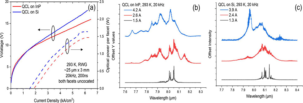
Figure 2: (a) Light output power and applied voltage versus current density of devices on InP and on Si substrate, at room temperature under pulsed operation. Emission spectra for lasers on (b) InP and (c) on Si, at different drive-current levels.
The threshold current density under pulsed operation was 22% lower on silicon than for a device grown on a bulk InP substrate in the same process run: in figures, 1.50kA/cm2 compared with 1.92kA/cm2, respectively. The researchers comment: “This may reflect a reduced silicon-dopant incorporation within the active-core superlattice layers due to either preexisting defects or a difference in the surface growth temperature for the silicon and InP substrates. In addition, non-uniform growth around the defect sites could potentially reduce the carrier mobility and tunneling efficiency, which would account for the higher series resistance observed for the devices grown on silicon.”
The higher series resistance was seen in the higher voltage needed to deliver a given current injection in the Si-based QCL. Despite the higher series resistance, the Si-based QCL also delivered a higher peak light output power: 1.64W and 1.47W for the Si- and InP-based devices, respectively. The corresponding slope efficiencies were 0.72W/A and 0.65W/A, and wall-plug efficiencies were 2.85% and 2.50%.
The spectral analysis of the emissions showed multiple modes in the wavelength range 7.6-8.3 μm. The largest peaks were around 8.1 μm and 8.0 μm for the InP- and Si-based devices, respectively. These wavelengths are a little shorter than the 8.2 μm design target. The researchers suggest that the differences could be due to local growth variations affecting layer thickness, as indicated in x-ray diffraction analyses.
The performance measured at various heat-sink temperatures between 293K and 353K gave characteristic temperatures for the degradations of threshold current (T0) and slope efficiency (T0) of 167K and 320K, respectively, for the QCL/Si. The QCL/InP had characteristics of 163K, T0, and 214K, T1.
MOCVD MBE IR quantum cascade lasers PICs
The author Mike Cooke is a freelance technology journalist who has worked in the semiconductor and advanced technology sectors since 1997.


