News: LEDs
10 August 2023
Understanding the impact of Auger recombination on InGaN LED efficiency
Researchers based in the UK and Ireland report that Auger recombination in indium gallium nitride (InGaN) multiple quantum wells (MQWs) is enhanced by carrier localization effects rather than defect assistance, according to their theoretical and experimental work [R. M. Barrett et al, ACS Photonics, published online 19 July 2023]. Auger recombination is seen as a major culprit in the droop in internal quantum efficiency (IQE) and external quantum efficiency (EQE) at high carrier concentrations, as seen at high current injection.
The team from University of Manchester in the UK, University College Cork in Ireland, and University of Cambridge in the UK, comment: “Good quantitative agreement between measurement and calculated IQE has now been demonstrated, showing that Auger recombination, enhanced by the localization of carriers but without any defect assistance, is sufficient to explain droop in the green-emitting QWs studied here.”
They add: “The peak IQE values of ~70% reported here under resonant excitation for samples that are designed to vary in point defect density and elsewhere show that there is limited scope for further improvement of maximum recombination efficiency within the active region of green-emitting QWs.”
The team thus believes that the focus should be on reducing expected carrier densities in LED operation towards the region of peak IQE. Although one might expect non-polar and semi-polar crystal orientation to improve droop effects, due to a faster recombination rate (sub-ns, as opposed to 10-100ns in the c-plane structures studied), this has not been realized experimentally.
The team suggests that there is more scope for improvement from focusing on aspects other than recombination within the active region: “For instance, improving the efficiency and homogeneity of carrier injection into the active region or reducing current leakage is likely to yield greater increases in EQE. This work also indicates that the most productive route to reducing droop is to target active region designs that reduce carrier density in individual QWs, such as the increased QW area or QW number or a more even distribution of carriers between QWs, rather than trying to reduce Shockley–Read–Hall (SRH) recombination in the active region.”
LEDs work by injecting electrons and holes into an active region where they recombine, releasing their energy as photons. Unfortunately there are other ways to release their energy. One way is through intermediate energy levels provided by defects — a process described by the Shockley–Read–Hall recombination mechanism. Another way is for an electron–hole pair to transfer their energy by give a kick to another carrier — Auger recombination. These SRH and Auger processes sap the desired effect of emitting photons in a desired wavelength range.
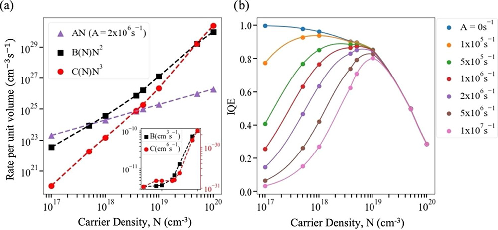
The ABC model commonly used to describe these effects attributes the rates of these processes to a linear (SRH, AN), quadratic (radiation of photons, BN2), and cubic (Auger, CN3) dependence on the carrier density (N). The internal quantum efficiency (IQE), as measured usually in luminescence experiments, is the ratio of recombination into photons (BN2) to the total recombination process (AN+BN2+CN3).
The rationale for the powers is that SRH depends on a single carrier, hence the single power, radiation on two carriers, so a double power, and Auger on three carriers... These indeed are the expected behaviors at low carrier densities, but other effects come into play at higher concentrations, and one expects a functional dependence of the ABC coefficients on N (Figure 1).

Figure 1: (a) SRH (AN), radiative (B(N)N2), and Auger (C(N)N3) recombination rates for a 15% indium, 3nm-wide (In,Ga)N/GaN QW. B(N) and C(N) from the group’s theoretical calculations. A coefficient is taken as constant based on literature. Inset: B(N) and C(N), averaged over two microscopic alloy configurations. (b) Calculated IQE curves for range of SRH A coefficients.
The team used theoretical ‘tight-binding’ calculations, which involved modeling about 82,000 atoms to find the expected alloy fluctuations and corresponding carrier localization effects.
To validate the theory, the researchers studied 5-period InGaN multiple quantum wells, with the wells grown at three different temperatures — 716°C, 706°C and 698°C. One expects the lower-temperature growth to result in a higher defect density in the wells, and hence higher rates of SRH recombination.
Another effect impacts the higher-growth-temperature samples: larger gross well width fluctuations (GWWFs). The team comments: “These GWWFs are expected to reduce the vulnerability of the QWs to recombination at point defects.” This again reduces the expected SRH rate from samples processed at high growth temperature.
The structures were grown by metal-organic chemical vapor deposition on GaN/sapphire templates. The GaN pseudo-substrate layer was around 4 μm thick. The wells had an estimated indium content of 17%. The InGaN wells were 3nm, and the GaN barriers were 7nm. The GaN barriers were grown using two temperature steps.
Pulsed photoluminescence was used to study the samples. The excitation wavelength of 400nm came from frequency-doubled titanium-doped sapphire (Ti:sapphire) laser. The pulse width was 150fs, delivered at 250kHz repetition rate. The excitation spot was 20 μm diameter with an energy density per pulse in the range 1.5–650 μJ/cm2. Emissions were collected from the center area over a 5 μm diameter for 700ns after the pulse.
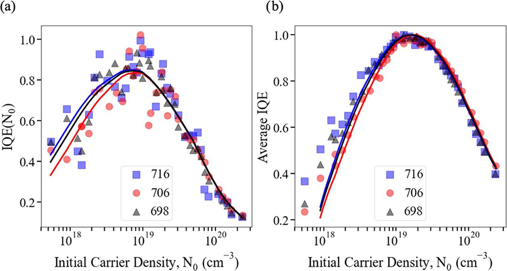
By studying the time-dependence of the luminescence, and relating the emitted radiation to the decay in the carrier concentration, the team extracted the relation of IQE (Figure 2) to the initial carrier concentration (N0). The larger scatter in the data was the result of the need to numerically differentiate in the extraction procedure.

Figure 2: Comparison of calculated (lines) and experimentally measured (symbols) values of (a) IQE and (b) average IQE during pulse. For both (a) and (b), experimental data has been scaled vertically to fit calculated values since measurements only determine relative, not absolute, IQE. Each sample labeled by growth temperature in °C.
The researchers point out that the behavior above 1019/cm3 carrier concentration effectively does not involve any fitting parameters (except for determining N0). The range for A derived from the lower carrier densities was 2–4x10⁶/s.
The author Mike Cooke is a freelance technology journalist who has worked in the semiconductor and advanced technology sectors since 1997.


