News: LEDs
24 August 2023
GaN:AlN superlattice UVC LEDs boost light extraction
Silanna UV in Australia reports on the use of gallium nitride:aluminium nitride (GaN:AlN) short-period superlattices (SPSLs) to improve the performance of far-ultraviolet-C (UVC) light-emitting diodes [Jordan Nicholls et al, Appl. Phys. Lett., v123, p051105, 2023]. The team claims a record radiant flux of 17.4mW for a far-UVC LED grown on sapphire.
Far-UVC light sources are sought for disinfection and sterilization efforts, such as those seen during the COVID-19 pandemic. The Silanna researchers comment: “The far-UVC wavelengths below 240nm are an extremely attractive option for this; light in this range has difficulty penetrating past the outmost layers of skin (the epidermis), and so exposure poses a reduced cancer risk.”
Although AlGaN LEDs are seen as a route to low-cost, compact UVC sources, there are a number of challenges to overcome. In particular, as the aluminium content of AlGaN increases, the generated light becomes more difficult to extract, since the recombination process emits photons into transverse magnetic (TM), rather than transverse electric (TE), modes. The light is then predominantly emitted, therefore, parallel and not perpendicular to the device layers. A further problem for high-Al-content AlGaN is poor doping efficiency.
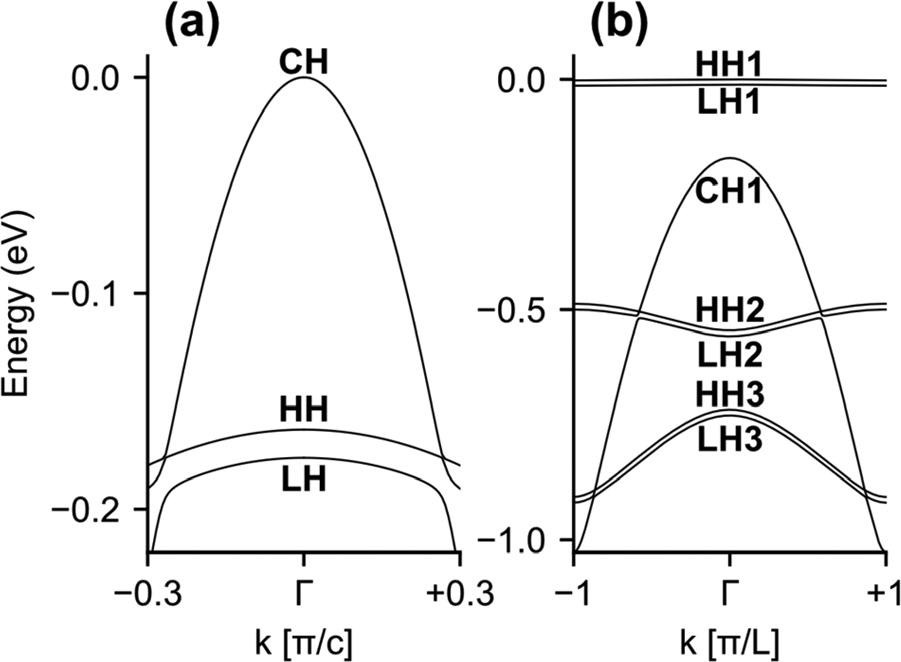
The light extraction problem is related to the ordering of the valence bands (Figure 1). In GaN, where light emission tends to be perpendicular to the device layers, the heavy-hole (HH) band is the highest energy level into which recombination of electrons from the conduction band predominantly takes place. In high Al-content AlGaN, by contrast, the crystal-field split-off hole (CH) band is the highest. Recombination into this band emits into TM modes.

Figure 1: Valence-band energy-quasimomentum (E-k) diagrams along the c-axis, as calculated by 6x6 k.p theory for (a) bulk Al0.8Ga0.2N and (b) 1:4 monolayer GaN:AlN short-period superlattice (SPSL) (period L).
The Silanna approach is to use SPSL structures to restore a HH mini-band, HH1, as the highest energy level, enabling TE light extraction. The SPSLs also ease doping efficiency problems. Rather than replace just one section of the device structure with an SPSL, the Silanna team used SPSLs almost throughout the entire epitaxial material layers.
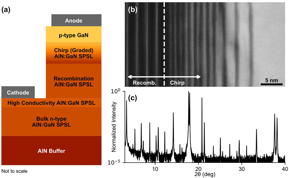
The AlN:GaN short-period superlattice (SPSL) LED material was grown by plasma-assisted molecular beam epitaxy (PAMBE) on a 6-inch sapphire substrate (Figure 2). The material was pseudomorphically strained to the underlying 400nm AlN buffer.

Figure 2: (a) Basic device structure of SPSL UV LEDs. (b) Transmission electron microscope image at interface between recombination and chirp regions. (c) X-ray diffraction x-2h scan of SPSL grown on AlN buffer.
The SPSLs consisted of alternating GaN and AlN layers. The thicknesses of these layers were varied to give different effective Al contents of the III–nitride material, and hence target wavelengths of the LEDs.
The 80nm/36-period recombination and 450nm bulk n-type regions of the device were separated by a 50nm high-conductivity region with a lower Al-content of 1:4 monolayers of GaN:AlN, giving an effective 80% Al over the 37 periods. The use of SPSL structure reduced the resistivity by a factor of three relative to values reported for bulk Al0.8G0.2N material. The recombination/bulk regions had approximately 93–98% Al, targeting 229–240nm wavelengths.
The final regions of the device consisted of a 20nm chirped/graded layer transitioning with increasing GaN layer thickness to the 40nm p-type GaN cap layer.
The researchers comment: “The purpose of the chirp layer was to improve hole injection from the much lower-bandgap GaN into the SPSL recombination region. It also serves as an electron-blocking layer to limit electrons overshooting past the recombination layer.”
The ionized acceptor concentration in the cap was of order 1x10¹⁹/cm3. The ionized donor concentration in the high-conductivity SPSL layer was estimated at 8x10¹⁹/cm3.
The material was fabricated into passivated mesa LEDs with titanium/aluminium contacts. The optoelectronic measurements were made using a 2-inch integrating sphere on the underside on the wafer.
The wavelength and power performance of the devices was uniform across the wafers. However, the electrical performance was less uniform. The team explains: “This is because the series resistance and, hence, the electrical characteristics are influenced by the etching and metallization processes, rather than solely the MBE growth process.”
A wafer with 233 ±1nm-wavelength devices had a yield of 10,763 LEDs. For the inner 4-inches of the wafer, the wavelength standard deviation was just 0.16nm. The average optical power output at 20mA injection was 0.2W for this inner section. The standard deviation of the drive voltage at 20mA was less than 0.16V for the devices more than half an inch away from the edge of the wafer.
The researchers comment: “Given that we can produce a greater than 4-inch area of consistent performance, our MBE-grown SPSL LED approach is one of the most promising from a production throughput and yield prospective.”
The team also packaged the 1mmx1mm singulated LEDs with electrostatic discharge protection from a commercial Zener diode shunt. The LEDs were thinned to 275μm before being packaged in AlN ceramic material. The measurements were made in a 6-inch integrating sphere (Figure 3).

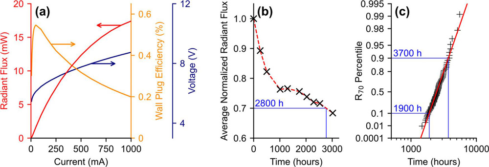
Figure 3: (a) Typical light output power, wall-plug efficiency, and voltage versus current injection for 236nm-wavelength device. (b) Lifetime performance for single device when operated at 20mA continuous current for 3000 hours, according to TM21 standard. (c) R70 percentiles for 80 packaged devices.
A typical packaged device reached 0.55% wall-plug efficiency (0.55%) at 50mA injection. According to the team, only one other group has reported a higher WPE, of 0.63%, for a 234nm-wavelength LED.
The radiant flux at the 0.55% peak efficiency was 1.7mW. The light output at 1A was 17.4mW. The researchers comment: “Although this is significantly beyond the intended drive current, this is the highest reported radiant flux for a far-UVC LED grown on a sapphire substrate.”
Although similar powers can be achieved for devices grown on AlN substrates, these are more expensive and smaller diameter. “Our ability to achieve comparable performance while using the more cost-effective sapphire is, therefore, an important milestone toward viable commercialization of far-UVC LED technology,” the team writes.
The lifetimes to 70% of the initial radiant flux (R70) were measured for 80 devices. A typical device had an R70 of 2800h, of which the researchers comment that “these are the longest-lived of any LEDs (which emit below 240nm) measured to date”.
The team used normal operating conditions (25°C, 20mA current) as specified in the TM21 standard. Other groups use higher currents to speed the aging process, which makes a true comparison difficult. One other group using the TM21 standard achieved an R70 of 1500h, significantly less than for the Silanna UV device.
The researchers also suggest that using a burn-in period to weed out weak devices could extend the lifetime to 7000h.
GaN:AlN superlattice UVC LEDs UVC LEDs GaN AlN AlGaN
https://doi.org/10.1063/5.0160177
The author Mike Cooke is a freelance technology journalist who has worked in the semiconductor and advanced technology sectors since 1997.


